Understanding Flash: Blocks, Pages and Program / Erases
https://flashdba.com/2014/06/20/understanding-flash-blocks-pages-and-program-erases/
In the last post on this subject I described the invention of NAND flash and the way in which erase operations affect larger areas than write operations. Let’s have a look at this in more detail and see what actually happens. First of all, we need to know our way around the different entities on a flash chip (or “package“), which are: the die, the plane, the block and the page:

NAND Flash Die Layout (image courtesy of AnandTech)
Note: What follows is a high-level description of the generic behaviour of flash. There are thousands of different NAND chips available, each potentially with slightly different instruction sets, block/page sizes, performance characteristics etc.
- The package is the memory chip, i.e. the black rectangle with little electrical connectors sticking out of it. If you look at an SSD, a flash card or the internals of a flash array you will see many flash packages, each of which is produced by one of the big flash manufacturers: Toshiba, Samsung, Micron, Intel, SanDisk, SK Hynix. These are the only companies with the multi-billion dollar fabrication plants necessary to make NAND flash.
- Each package contains one or more dies (for example one, two, or four). The die is the smallest unit that can independently execute commands or report status.
- Each die contains one or more planes (usually one or two). Identical, concurrent operations can take place on each plane, although with some restrictions.
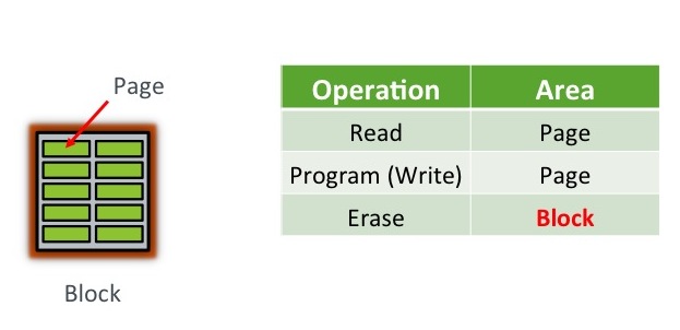
- Each plane contains a number of blocks, which are the smallest unit that can be erased. Remember that, it’s really important.
- Each block contains a number of pages, which are the smallest unit that can be programmed (i.e. written to).
The important bit here is that program operations (i.e. writes) take place to a page, which might typically be 8-16KB in size, while erase operations take place to a block, which might be 4-8MB in size. Since a block needs to be erased before it can be programmed again (*sort of, I’m generalising to make this easier), all of the pages in a block need to be candidates for erasure before this can happen.
Program / Erase Cycles
When your flash device arrives fresh from the vendor, all of the pages are “empty”. The first thing you will want to do, I’m sure, is write some data to them – which in the world of memory chips we call a program operation. As discussed, these program operations take place at the page level. You can then read your fresh data back out again with readoperations, which also take place at the page level. [Having said that, the instruction to read a page places the data from that page in a memory register, so your reading process can in fact then selectively access subsets of the page if it desires – but maybe that’s going into too much detail…]
 Where it gets interesting is if you want to update the data you just wrote. There is no update operation for flash, no undo or rewind mechanism for changing what is currently in place, just the erase operation. It’s a little bit like an etch-a-sketch, in that you can continue to turn the dials and make white sections of screen go black, but you cannot turn black sections of screen to white again without erasing the entire screen.
 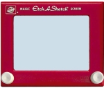 An erase operation on a flash chip clears the data from all pages in the block, so if some of the other pages contain active data (stuff you want to keep) you either have to copy it elsewhere first or hold off from doing the erase.
In fact, that second option (don’t erase just yet) makes the most sense, because the blocks on a flash chip can only tolerate a limited number of program and erase options (known as the program erase cycle or PE cycle because for obvious reasons they follow each other in turn). If you were to erase the block every time you wanted to change the contents of a page, your flash would wear out very quickly.
So a far better alternative is to simply mark the old page (containing the unchanged data) as INVALID and then write the new, changed data to an empty page. All that is required now is a mechanism for pointing any subsequent access operations to the new page and a way of tracking invalid pages so that, at some point, they can be “recycled”.

Updating a page in NAND flash. Note that the new page location does not need to be within the same block, or even the same flash die. It is shown in the same block here purely for ease of drawing.
This “mechanism” is known as the flash translation layer and it has responsibility for these tasks as well as a number of others. We’ll come back to it in subsequent posts because it is a real differentiator between flash products. For now though, think about the way the device is filling up with data. Although we’ve delayed issuing erase operations by cleverly moving data to different pages, at some point clearly there will be no empty pages left and erases will become essential. This is where the bad news comes in: it takes many times longer to perform an erase than it does to perform a read or program. And that clearly has consequences for performance if not managed correctly.
In the next post we’ll look at the differences in time taken to perform reads, programs and erases – which first requires looking at the different types of flash available: SLC, MLC and TLC…
Understanding Flash: Blocks, Pages and Program / Erases的更多相关文章
- Understanding Objective-C Blocks
The aim of this tutorial is to give a gentle introduction to Objective-C blocks while paying special ...
- 一些有趣的B+树优化实验
作为目前数据库引擎的两种主要数据结构,LSM-tree和B+-tree在业界已经有非常广泛的研究.相比B+-tree,LSM-tree牺牲一定的读性能以换取更小的写放大以及更低的存储成本,但这必须建立 ...
- A New 3-bit Programming Algorithm using SLC-to-TLC Migration for 8MBs High Performance TLC NAND Flash Memory
背景 1.2012年左右的数据SLC.MLC.TLC闪存芯片的区别:SLC = Single-Level Cell ,即1bit/cell,速度快寿命长,价格超贵(约MLC 3倍以上的价格),约10万 ...
- UEFI Bootable USB Flash Drive - Create in Windows(WIN7 WIN8)
How to Create a Bootable UEFI USB Flash Drive for Installing Windows 7, Windows 8, or Windows 8.1 In ...
- [翻译]理解Ruby中的blocks,Procs和lambda
原文出处:Understanding Ruby Blocks, Procs and Lambdas blocks,Procs和lambda(在编程领域被称为闭包)是Ruby中很强大的特性,也是最容易引 ...
- [转]Flash Socket通信的安全策略
昨天做测试的时候遇到一个问题,做好的SWF在Flash AS3中调试通过,但是发布到html中之后就无法得到数据了.查了一些资料之后找到了解决办法.这里感谢 剑心 提供帮助,以及同事若水三千提供Jav ...
- Core Java Volume I — 3.1. A Simple Java Program
Let’s look more closely at one of the simplest Java programs you can have—one that simply prints a m ...
- Apache Flex + Adobe Flash Builder环境配置
在开始学习Flex之前,需要配置开发环境.Apache Flex SDK包含了你开发所需要的东西,当然除了集成开发环境(Integrated Development Environment,IDE). ...
- Flash Socket通信的安全策略问题 843端口
1.问题描述 将flash发布为html格式后,加载页面后,swf无法与服务器进行socket通信.Flash端显示的错误为:securityErrorHandler信息: [Securi ...
随机推荐
- Django中使用Celery,定制应用程序中定义的shared_task未在定期任务管理页面的注册任务中显示
解决办法: 在项目 proj/proj/celery.py文件中,看到下面这行配置: celery_app.config_from_object('django.conf:settings', nam ...
- SkinTK编译使用
简介 MFC这个东西已经落伍了,不建议使用.我就是吃饱了撑着,还在折腾这个. 平时写点带界面的小程序一般都用Qt来做,简单好用,也很容易做的比较漂亮.我觉得唯一一个算不得多大缺点的缺点就是Qt体积太大 ...
- Long polling failed, will retry in 16 seconds. appId: zeus-guard, cluster: default, namespaces: application, long polling url: null, reason: Get config services failed from···
当dubbo应用启动之前, 如果apollo 未启动好,那么我们dubbo应用会一直等待,直到apollo准备就绪,注意其中轮询时间是从1,2,3,4,8,14,32, 方式一直增长,单位是s.
- Git教程学习(四)
12. 分支管理场景 多人协同工作时,你在优化代码X,需要较长时间才能完成,未完成之前会影响整体代码的使用.于是写完的代码不能提交到版本库,提交就会影响别人使用整体的代码.不提交你就失去了git的版本 ...
- Spring开发工具Spring Tools Suite(STS)
The Spring Tool Suite is an Eclipse-based development environment that is customized for developing ...
- JPA+Hibernate 3.3 ——增删改查
1. 查找对象 1) 用find()方法查找对象 public void getPerson(){ EntityManagerFactory factory = Persistence. ...
- 一篇文章掌握RequireJS常用知识
本文采取循序渐进的方式,从理论到实践,从RequireJS官方API文档中,总结出在使用RequireJS过程中最常用的一些用法,并对文档中不够清晰具体的内容,加以例证和分析,分享给大家供大家参考,具 ...
- Multiplication of numbers
Questin: There is an array A[N] of N numbers. You have to compose an array Output[N] such that Outpu ...
- idea 添加项目到svn
version control 改变项目为svn管理 如图 分享 share dic 添加新地址 share 剩下的 就是设置忽略目录 提交
- HDOJ 1393 Weird Clock(明确题意就简单了)
Problem Description A weird clock marked from 0 to 59 has only a minute hand. It won't move until a ...