基础003_V7-Memory Resources
一、综述
参考ug473.pdf。
常用Memory 资源:

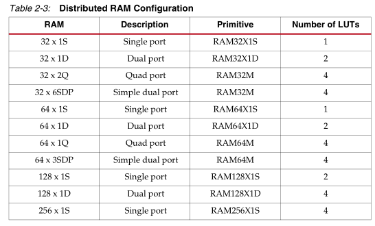
在IP核中,Block memory(distributed memory为CLB中的资源):

通常选用Native,而不用AXI接口:
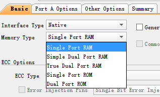
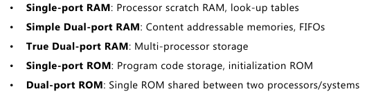
Block RAM可配置单端口RAM、伪双端口RAM、双端口RAM、单端口ROM、双端口ROM、FIFO。
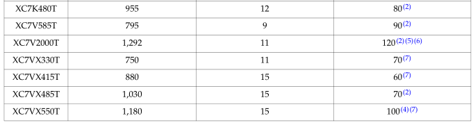
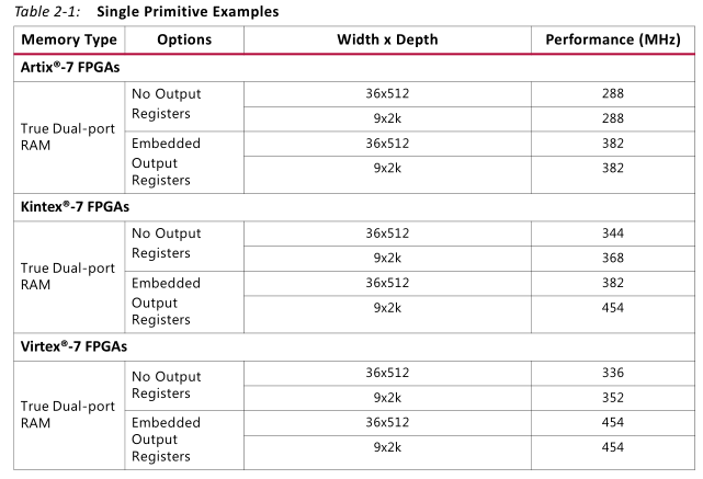
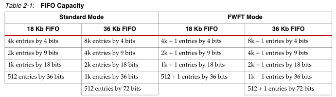
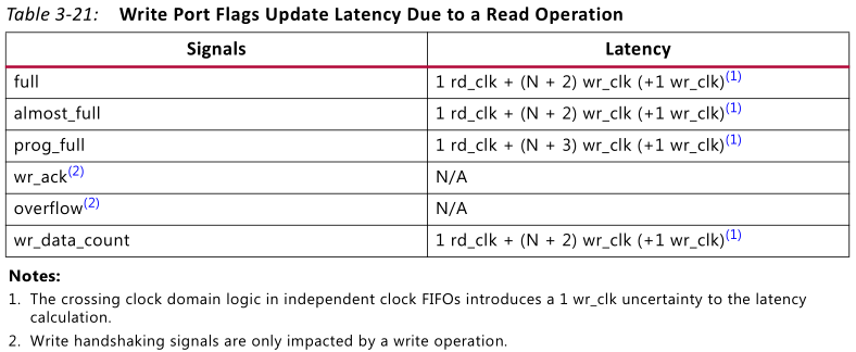
各个模式调用时可承受的最高频率,参考pg058.pdf:
二、主要功能
学习资源: http://www.asic-world.com/examples/verilog/memories.html

A-RAM/ROM
主要功能:
每一个Block RAM都可配置为1个36Kb的BRAM或1个36Kb的FIFO;同时也可以将其配置为2个单独的18Kb的BRAM或1个18KbBRAM + 1个18Kb的BRAM。
为什么是18k而不是16k(2的整次幂)?因为每8bit一个校验位。2*8 + 2 =18bit。
结论:无论是单端口RAM、伪双端口RAM还是双端口RAM,他们都只有一块Memory。
Single-port RAM:
同步示例:
module ram_sp_sr_sw (

clk         , // Clock Input

address     , // Address Input

data        , // Data bi-directional

cs          , // Chip Select

we          , // Write Enable/Read Enable

oe            // Output Enable

);

parameter DATA_WIDTH = 8 ;

parameter ADDR_WIDTH = 8 ;

parameter RAM_DEPTH = 1 << ADDR_WIDTH;

//--------------Input Ports-----------------------

input                  clk         ;

input [ADDR_WIDTH-1:0] address     ;

input                  cs          ;

input                  we          ;

input                  oe          ;

//--------------Inout Ports-----------------------

inout [DATA_WIDTH-1:0]  data       ;

//--------------Internal variables----------------

reg [DATA_WIDTH-1:0] data_out ;

reg [DATA_WIDTH-1:0] mem [0:RAM_DEPTH-1];

reg                  oe_r;

//--------------Code Starts Here------------------

// Tri-State Buffer control

// output : When we = 0, oe = 1, cs = 1

assign data = (cs && oe && !we) ? data_out : 8'bz;

// Memory Write Block

// Write Operation : When we = 1, cs = 1

always @ (posedge clk)

begin : MEM_WRITE

   if ( cs && we ) begin

       mem[address] = data;

   end

end

// Memory Read Block

// Read Operation : When we = 0, oe = 1, cs = 1

always @ (posedge clk)

begin : MEM_READ

  if (cs && !we && oe) begin

    data_out = mem[address];

    oe_r = 1;

  end else begin

    oe_r = 0;

  end

end

endmodule // End of Module ram_sp_sr_sw
异步(异步读、同步写)示例:
module ram_sp_ar_sw (

clk         , // Clock Input

address     , // Address Input

data        , // Data bi-directional

cs          , // Chip Select

we          , // Write Enable/Read Enable

oe            // Output Enable

);

parameter DATA_WIDTH = 8 ;

parameter ADDR_WIDTH = 8 ;

parameter RAM_DEPTH = 1 << ADDR_WIDTH;

//--------------Input Ports-----------------------

input                                     clk          ;

input [ADDR_WIDTH-1:0] address ;

input                                     cs           ;

input                                     we          ;

input                                     oe           ;

//--------------Inout Ports-----------------------

inout [DATA_WIDTH-1:0]  data       ;

//--------------Internal variables----------------

reg [DATA_WIDTH-1:0]   data_out ;

reg [DATA_WIDTH-1:0] mem [0:RAM_DEPTH-1];

//--------------Code Starts Here------------------

// Tri-State Buffer control

// output : When we = 0, oe = 1, cs = 1

assign data = (cs && oe && !we) ? data_out : 8'bz;

// Memory Write Block

// Write Operation : When we = 1, cs = 1

always @ (posedge clk)

begin : MEM_WRITE

   if ( cs && we ) begin

       mem[address] = data;

   end

end

// Memory Read Block

// Read Operation : When we = 0, oe = 1, cs = 1

always @ (address or cs or we or oe)

begin : MEM_READ

    if (cs && !we && oe) begin

         data_out = mem[address];

    end

end

endmodule // End of Module ram_sp_ar_sw
对应电路:
可以看出2^8 = 256由4个64拼接拼接而成:
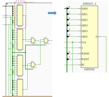
这里其实调用的是CLB中SliceM下的Distributed RAM资源:
B-FIFO
FIFO的能力:
FIFO的IP核使用,具体可参考:pg057.pdf。
FIFO可调用shift reg、distributed RAM、Block RAM、BulitIn FIFO,关于使用,xilinx论坛有相关说法:
Q:
From PG057 (Fifo generator) I understand FIFO's can be implemented in 4 ways, using :
- block RAM
- distributed RAM
- shift register
- built-in FIFO (using FIFO18 / FIFO36)
is there any simple document / app note / overview describing on what basis you typically decide between the 4 implementations. What are the main tradeoffs, advantages, ... of each underlying memory type used?
I can imagine a few, but not sure if these are correct and complete :
- block RAM is interesting for large, deep fifo's
- distributed RAM is interesting for smaller fifo's
- shift register is interesting for smaller fifo's, with short word width
- built-in FIFO allow for the fastest fifo's
but that's just intuition ... so any corrections or further insights are welcome here!
A:
Its based your application , requirement and available resources in your target FPGA. The most of the points you mention correct. I would recommend you to refer target FPGA resource guide LUTs have lowest access time, FIFO18/FIFO36 good timing performance but require effort in design migration, BRAM very good for scalable memory requirement . You can also check about URAM/ultraram available in ultrascale devices
三、IP核调用
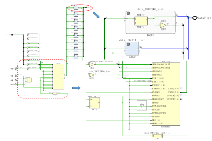
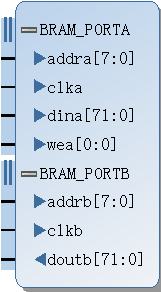
A-simple dual RAM
参考IP_bram笔记。
这里涉及到位宽的计算,以6通道,160MHz采样率,12bit有效位AD举例,现在需要转化为:240MHz的FPGA工作时钟。
12bit*6*160/240 = 48bit
位宽由12*6 = 72bit转化为48bit,:
- Port-A为写数据,width:位宽12*6 = 72bit,depth = 160
- Port-B为读数据,width:48bit,depth = 240
但Port-B的width只能是:72bit/(2^n),n = 0, ±1, ±2, ...,因此通常都是二次转化:
Step1:72*160 = 48*240 < x * 240,x = 72*2^n >48,此处n = 0;x工作在240MHz。
Step2:x * M = 48 * N,M、N都是整数。M = 1,N = 2,完成转化。
.png)
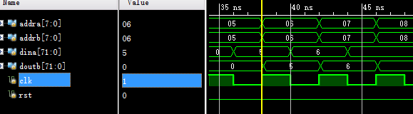
勾选primitive output register:
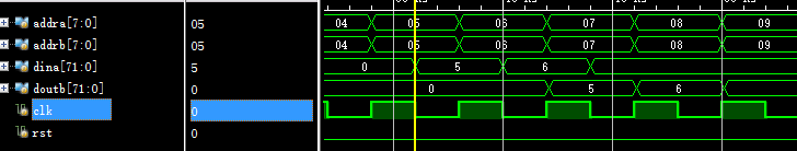
可见该选项延迟了1拍。
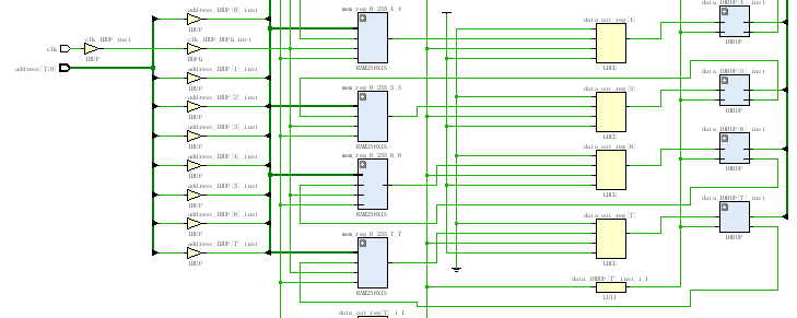
B-FIFO
主要参考:

关于IP核参数设置,可参考FIFO generator笔记。
与BRAM同样的例子,很多时候数据时钟域转换用dual-port RAM而不用FIFO,说是前者含地址,存在时延变量取数方便,但改为FIFO实现其实也可以,后者含有计数功能,同样可以进行定位。
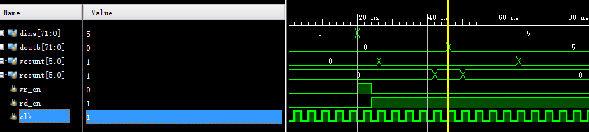
从读使能给出,到数据输出,经过6个周期,计算:
基础003_V7-Memory Resources的更多相关文章
- Understanding Virtual Memory
Understanding Virtual Memory by Norm Murray and Neil Horman Introduction Definitions The Life of a P ...
- DTrace to Troubleshoot Java Native Memory Problems
How to Use DTrace to Troubleshoot Java Native Memory Problems on Oracle Solaris 11 Hands-On Labs of ...
- Spring Boot Memory Performance
The Performance Zone is brought to you in partnership with New Relic. Quickly learn how to use Docke ...
- 再谈.net的堆和栈---.NET Memory Management Basics
.NET Memory Management Basics .NET memory management is designed so that the programmer is freed fro ...
- Allowing GPU memory growth
By default, TensorFlow maps nearly all of the GPU memory of all GPUs (subject to CUDA_VISIBLE_DEVICE ...
- CUDA ---- Memory Model
Memory kernel性能高低是不能单纯的从warp的执行上来解释的.比如之前博文涉及到的,将block的维度设置为warp大小的一半会导致load efficiency降低,这个问题无法用war ...
- Memory Leak Detection in C++
原文链接:http://www.linuxjournal.com/article/6556?page=0,0 An earlier article [“Memory Leak Detection in ...
- System and method for parallel execution of memory transactions using multiple memory models, including SSO, TSO, PSO and RMO
A data processor supports the use of multiple memory models by computer programs. At a device extern ...
- Move resources allocated using unmanaged interface to managed devm interface
转载:http://blog.csdn.net/swingboard/article/details/27207497 So today let’s talk about devm functio ...
- Find out when memory leaks are a concern and how to prevent them
Handling memory leaks in Java programs Find out when memory leaks are a concern and how to prevent t ...
随机推荐
- WIP 004 - Quote/Policy Search
Please create the search form Auto complete for first name and last name Related tables System_LOBs ...
- jqPlot图表插件学习之柱形图和旋转分类名称
一.准备工作 首先我们需要到官网下载所需的文件: 官网下载(笔者选择的是jquery.jqplot.1.0.8r1250.zip这个版本) 然后读者需要根据自己的情况新建一个项目并且按照如下的方式加载 ...
- Redis从入门到精通:中级篇(转)
原文链接:http://www.cnblogs.com/xrq730/p/8944539.html,转载请注明出处,谢谢 本文目录 上一篇文章以认识Redis为主,写了Redis系列的第一篇,现在开启 ...
- VS编译 x64版本zlib库
编译的过程倒也不是很难.我把编译的源码和脚本及说明都放在gitee上了. 详细的可以见这里 https://gitee.com/solym/zlib-1.2.11.git 可以参考这些文章 win10 ...
- JS修改当前控件样式&为控件追加事件
先搁这吧,今天太晚了,以后再加注释和修整吧.不幸搜到的朋友就别看了 <%@ Page Language="vb" AutoEventWireup="false&qu ...
- scala object 转Class Scala强制 类型转换
scala object 转Class Scala强制类型转换 asInstanceOf[T] 将对象类型强制转换为T类型. 还是由于泛型存在类型擦除的原因,1.asInstanceOf[Stri ...
- Vivaldi浏览器媲美Chrome
Vivaldi跨平台的浏览器,很好的兼容性...基本上跟Chrome一个层次的... 好的东西,用一次就明白!好酒,酒香巷子深... Download: https://vivaldi.com/dow ...
- ftp相关常用命令
工欲善其事必先利其器 00.FTP常用命令 01.SFTP命令 sftp user@ip:/tmp
- ThinkPHP学习(二)
书接前文. 我想前台填写内容,然后在后台保存一下,规划了一下前台要录入的内容,主要包括title.content两大内容.然后简单设计了一个前台页面(复杂的我得会啊),就在上篇文章的基础上直接加了: ...
- 工欲善其事,必先利其器 软件工具开发关键词 protractor自动化测试工具 RegexBuddy正则 CodeSmith,LightSwitch:代码生成 CheatEngine:玩游戏修改内存值必备神器 ApkIDE:Android反编译工具 Reflector:反编译dll动态链接库
工欲善其事,必先利其器 本文版权归翟士丹(Stan Zhai)和博客园共有,欢迎转载,但未经作者同意必须保留此段声明,且在文章页面明显位置给出原文链接,否则保留追究法律责任的权利. 原文地址:http ...