ADC In An FPGA
http://davidkessner.wordpress.com/2011/05/01/adc-in-an-fpga/
Geek Alert! What follows is very technical. It involves ADC’s, FPGA’s, and sophisticated electrical design. If this doesn’t sound like you then you can safely skip the rest of this blog post.
EDIT: Part 2 of this series is up. Read it here, when you’re done with Part 1, of course.
I’ve always had this crazy idea to implement an ADC (Analog to Digital Converter) in an FPGA. Recently I worked out a lot of the details, enough where I started to get concerned about future patent violations and associated legal issues. I’ve decided to post a summary of my work, as a record of prior art, just in case something actually comes from this. Along the way, some other geeks might be interested in this.
This ADC is supposed to be inexpensive– that’s the main goal. My requirements for this were to have no active external components. The idea is that if you already have an FPGA with some unused pins, and add some passive components then you could have a simple ADC for almost nothing. Along that line of thought, the logic inside the FPGA should also be super small.
These design parameters makes things quite difficult, and requires some out-of-the-box thinking. Normally one would consider the traditional ADC architectures and then shoehorn that into an FPGA. But after looking at them, I decided that none of them really fit the FPGA implementation very well. So instead of doing a top-down approach, I went with the bottom up.
At the core, all ADC’s rely on some sort of voltage comparator. In the FPGA, the only real comparator would be a differential input buffer. LVDS, for example. Of course, such a buffer has lots of bad behaviors like hysteresis– but that’s all we have to work with. The architecture I came up with should work around these issues.
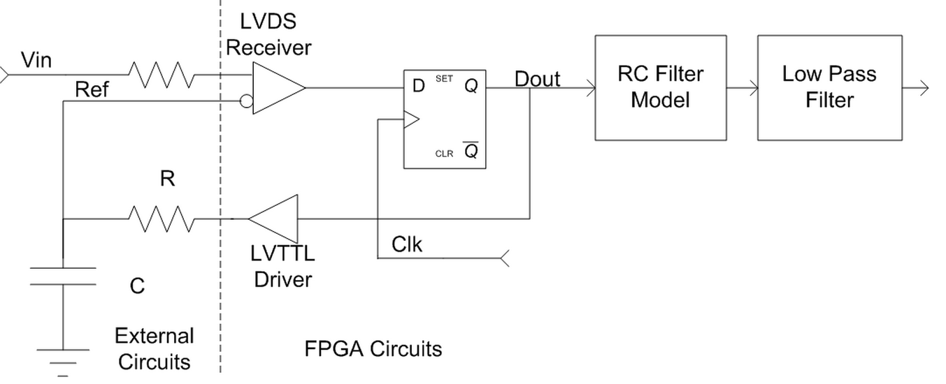
Below is a block diagram for my ADC, click on it to enlarge. For the moment, ignore the RC Filter Model and Low Pass Filter.

Normally, Ref would mostly track Vin. The LVDS receiver, used as a voltage comparator, senses if Ref is too high or too low, and feeds the external RC filter accordingly. There will be some ripple on Ref, which is mostly the result of the RC filter characteristics and the hysteresis of the LVDS receiver. Oddly enough, however, this ripple helps the circuit.
The RC Filter Model is simply a digital representation of the external RC filter. The output of this block is the voltage of the Ref signal (including all the ripple). The Low Pass Filter is there to smooth out the ripple on the RC Filter Model.
That’s it! Ok, the devil is in the details, but that’s most of it. I’ll get to some of those details, but let’s look at some waveforms.
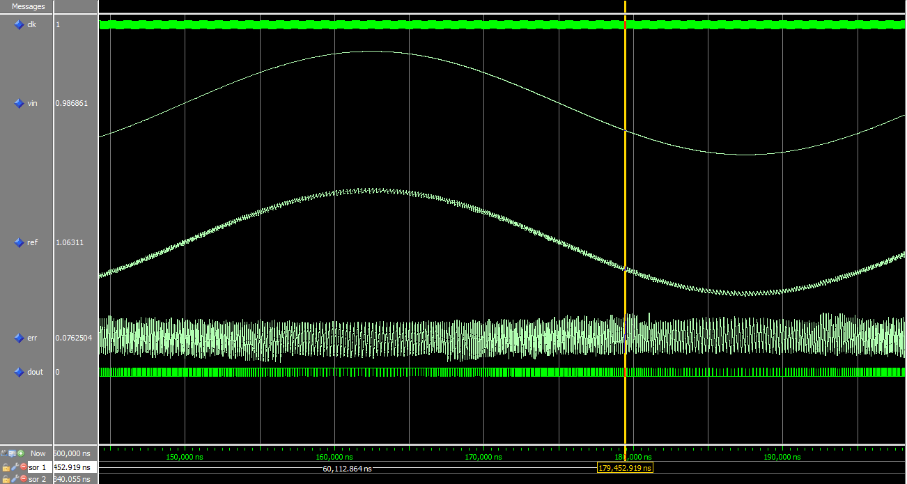
For these waveforms and unless otherwise said, Vin is a 10 KHz sine wave from 0.4v to 2.9v, C=220 pF, R=3.3K ohms, and the LVDS receiver hysteresis is 50 mV.

In the image above (click to enlarge), you’ll see Vin doing it’s thing with Ref tracking it. Of course Ref has the expected ripple. The Err signal is the difference between Vin and Ref, and has a swing of about +/- 65 mV. Dout and Clk are there, but when zoomed out this far you can’t see anything useful. Here is the same waveforms, but zoomed in a lot:

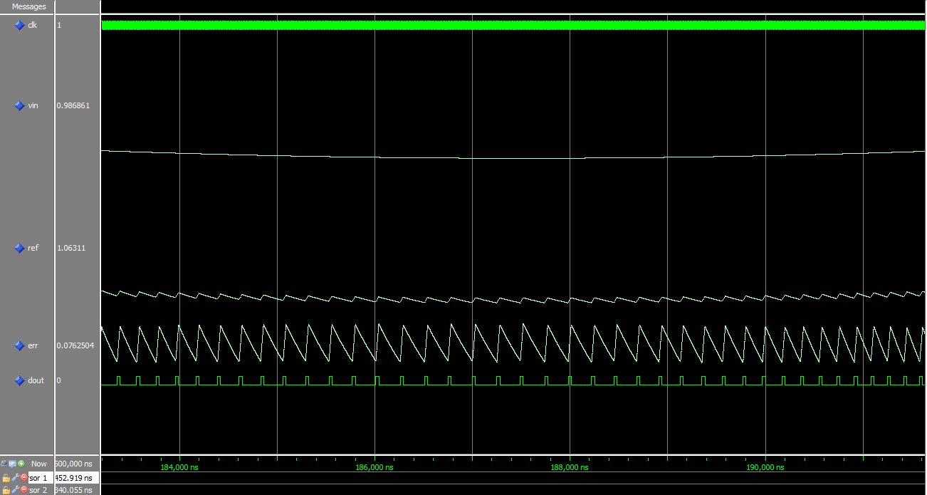
In this image you can clearly see the ripple, and resulting Err, on Ref. You can also see Dout. One thing that should be mentioned at this point is that Dout is not simply a PWM’d representation of Ref. As Ref changes voltage, the ability for Dout to charge/discharge the external cap changes due to the voltage across R. This image shows Ref when it’s at its lowest level, so Dout has an easy time driving Ref higher but has difficulty bringing it lower. This is shown as a change in slew rate on Err, fast rising edge and slow falling edge.
The LVDS hysteresis and RC time constant will effect the ripple frequency. Also, this frequency will slow down as Vin/Ref get closer to the power and ground rails. As a general rule, you want this ripple to be as high frequency as possible while still maintaining a somewhat analog appearance. I’ve found that 220 pF and 3.3K Ohms is about the shortest RC time constant that’s practical using LVDS and LVTTL.
The RC Filter Model sounds daunting at first, but isn’t too bad in reality. First, we’ll go over the math. The formula is this:
Ref_New= Ref_Current + (Dout-Ref_Current) * (1-exp(-T/RC))
Where Ref_New is the new value of Ref, Ref_Current is the current value of Ref, Dout is either 0.0 or 3.3 depending on the state of Dout, T is the clock period in seconds, R is in ohms, and C is in farads. The function exp(x) returns e to the power of x.
In the FPGA, it’s only the last part of that formula that’s hard, the “* (1-exp(-T/RC))” part. But on closer inspection it’s not that bad. Since T, R, & C do not change at runtime, the whole thing becomes a multiplication by a constant. That’s a good thing, because doing an exp() function in an FPGA is challenging and uses lots of logic.
That constant would normally be represented as fixed point. By careful selection of R and C, that constant can have very few ’1′ bits in it– maybe even a single ’1′ bit. This is super important. Fixed point multiplication by a number with a single ’1′ bit is the same as a bit-shift! And, as you know, a bit-shift in an FPGA takes no logic. If there are two ’1′ bits then it’s two shifts and an addition– still not bad. One of my goals in the near future is to write a program that will find combinations of T, R, and C that make the math easier. I’ve done something similar in the past and it works out really slick.
Another “optimization” is to scale the numbers. Instead of Ref being represented by a fixed point number from 0.0 to 3.3, it can be represented as 0.0 to 0.999999. In binary, that would be from “00000000″ to “11111111″. While that doesn’t make the math any easier, it does make the ADC somewhat independent of the I/O Standards used, and puts the ADC output in a more useful form.
The Low Pass Filter can be just about anything, depending on what quality of output you require. A simple averaging filter can be good enough for most things. For better performance, there are many types of IIR filters that would work well. I don’t recommend a FIR filter for this, due to the sample rates and the number of taps that you would need.
It’s a little preliminary to talk about performance of this ADC. I have simulated enough of this to know that the theory is sound, but I have not built an actual circuit or done an FFT analysis on the output. But based on what I’ve seen so far, it seems like a slam dunk to get 10 KHz bandwidth (20 KHz output sample rate) and 12-bit performance. Higher sample rates are possible with sacrificing rail to rail operation and bit resolution.
I should also mention that the same RC Filter Model can be used to make a nice DAC in an FPGA. Doing so would be better than using PWM or a first-order Delta Sigma modulator (similar to a Xilinx app note) in that the DAC settling time is faster, it has a more linear input to output response, and can operate with a faster RC time constant resulting in better frequency reponse.
So there you go! If you like this, let me know. Maybe I’ll have to post some VHDL code or something.
This is part 2 of “ADC In an FPGA”. If you have not read part 1, here it is.
Part 1 covered an overview of the ADC design. Part 2 is going to cover a small part of it, but in more detail. Specifically, the math around the RC filter model and how to optimize it to almost nothing.
The RC filter model is basically a chunk of logic inside the FPGA that attempts to predict what the external RC filter is actually doing, without directly measuring it. The math behind this is conceptually easy, so here’s the formula.
New_Voltage = Current_Voltage + (RC_Input_Voltage – Current_Voltage) * (1-exp(-T/RC))
Where:
T = Clock period, in seconds
R = Resistor, in ohms
C = Capacitor, in Farads
Current_Voltage = The current output voltage of the RC filter
RC_Input_Voltage = The output of the FPGA, going into the RC filter
New_Voltage = The output voltage of the RC filter after T seconds
exp() = The exponential function.
At first glance, this looks like it would be hard to implement in an FPGA, but rest assured that it isn’t.
The first optimization that we’re going to do is change “voltage” to be a value from 0.0 to 1.0. Basically, a percentage of the power rail voltage. So if our I/O Voltage is 3.3v then a value of 1.0 would represent a voltage of 3.3, and a value of 0.5 would represent 1.65 volts. This is super easy to do, all you do is change the definitions of the variables in the above formula. The new formula is:
New_Value = Current_Value + (RC_Input_Value – Current_Value) * (1-exp(-T/RC))
Where all of the “values” have a range of 0.0 to 1.0. And since the FPGA can only output ’0′ or ’1′, the acceptable values for RC_Input_Value can only be 0.0 or 1.0 and nothing in between.
Of course in the FPGA we would not be doing the math for this as floating point (“real” numbers in VHDL). That would be silly. Instead we’ll use the standard fixed point notation where (using a 4-bit vector for example) “0000″ would be a value of 0.0. “0111″ would be, essentially 1.0. “1000″ would be -1.0. And “0010″ would be +0.5.
The next thing to optimize is the ” * (1-exp(-T/RC))” part. It is important to note that since T, R, and C do not change once the design is done that this expression simplifies down to multiplication by a constant. In an FPGA, multiplication by an arbitrary constant is easy but can take up a lot of logic. Either it will use up some integer multiplier inside the FPGA, or end up as some crazy adder tree. Sometimes that’s appropriate, but we can do better.
So we don’t want to multiply by an arbitrary constant. But if our constant had only a single bit set in it, then our multiplication turns into a simple bit-shift, and a bit-shift in an FPGA takes no logic at all! We do have control over what R and C are, and to a lesser extent T. If we choose our R and C carefully then we can find a constant with only 1 bit set– and our multiplication becomes dirt simple.
Finding the appropriate R and C is not simple. If you did it by hand it would take lots of tedious calculations. Fortunately, computers are good at that sort of thing. I wrote a program that, when given T, will calculate all R’s and C’s that have a nice constant value associated with them.
It works like this: Let’s assume that R and C are 3.16K and 200 pF, and our T is 10 nS. From that we can calculate that our constant is 0.015698261559. When we convert it to our fixed point representation, we get 0x0202668F, assuming 32 bit signed numbers. If we then chop off all but the first ’1′ bit, we get 0×02000000. Now, 0×02000000 looks a lot different than 0x0202668F, but if you convert it back into normal floating point (0.015625000000) you’ll see that it is about 0.47% off from the original number. In the grand scheme of things 0.47% is not a lot considering the resistor has a tolerance of 1% and the cap is much worse.
My program does this for all combinations of R and C, and spits out the combinations that are within 1% of the ideal value. Click on adc_constants to get an Excel file with the most popular clock frequencies already calculated. Inside the file are multiple sheets, one for each clock frequency. Each sheet has the following columns:
R — The resistor value
C — The capacitor value
Const(ideal) — The ideal value for our (1-exp(-T/RC)) constant, without rounding and stuff.
Const(int) — The 32-bit integer representation of our constant, in hex, and after all the bit mangling.
Const(float) — The floating point version of Const(int), after bit mangling.
Const Err– The error between Const(float) and Const(ideal).
n_bits — The number of ’1′ bits in Const(int)
rc — The RC time constant for R and C
The easiest way to use this file is to go to the sheet with your clock frequency, and pick out an RC combination that is close to what you want. I strongly suggest using the Excel sort data function to put the data into an order that makes life easier. By default, it is sorted by R and then C. But sorting by rc and then by Const Err could be useful too. Either way, pick out an RC and go to town!
I should also note that the table does not include resistors smaller than 3K ohms. This is intentional. If the resistor is any smaller then the load on the FPGA output pin is too high to allow the output to switch rail to rail. Rail to rail outputs is essential to keeping everyone sane.
For some reason, this blog software doesn’t allow me to post Zip files, EXE’s, or normal text files. Once I figure out how to do this I can post the source code and EXE for the software that generates these tables. With that software, you can calculate RC’s for odd-ball clock frequencies or constants with more than just 1 bit set in it.
Once the dust settles, our original formula has turned into a simple bit shift and addition. Ya can’t get much simpler than that!
Next ADC post will cover more of the low pass filter, and how to optimize that one to death as well.
ADC In An FPGA的更多相关文章
- FPGA LVDS I/O as an Analog Programmable Comparator
http://www.eetimes.com/author.asp?section_id=36&doc_id=1320289 Seeing the new ADC IP being bandi ...
- 高速AD中的LVDS和FPGA
通常情况下,模拟输入信号通过高速ADC的量化输出的数字信号需要交给FPGA进行处理.如果高速ADC采用LVDS输出,那么经量化处理过的数字信号将会有非常多的LVDS数据差分对.而LVDS数据接收端,接 ...
- 数字信号处理专题(1)——DDS函数发生器环路Demo
一.前言 会FPGA硬件描述语言.设计思想和接口协议,掌握些基本的算法是非常重要的,因此开设本专题探讨些基于AD DA数字信号处理系统的一些简单算法,在数字通信 信号分析与检测等领域都会或多或少有应用 ...
- FPGA高速ADC接口实战——250MSPS采样率ADC9481
一.前言 最近忙于硕士毕业设计和论文,没有太多时间编写博客,现总结下之前在某个项目中用到的一个高速ADC接口设计部分.ADC这一器件经常用于无线通信.传感.测试测量等领域.目前数字系统对高速数据采集的 ...
- 【资讯】天啦鲁,这十余款创客设计居然由FPGA搞定 [转]
按理说‘高大上’的FPGA,多出现在航天航空(如火星探测器).通信(如基站.数据中心).测试测量等高端应用场景.但麦迪却也发现,近期,在很多创客的作品内部都有FPGA的影子.这或许也从侧面看出,打从总 ...
- 基于FPGA的线阵CCD图像测量系统研究——笔记
本文是对基于FPGA的线阵CCD图像测量系统研究(作者:高尚)的阅读笔记 第一章绪论 1. 读读看 读了前面的摘要依然没有看懂作者要做什么.接着往下读....终于看到了一个字眼“基于机器视觉的图像测量 ...
- 【小梅哥FPGA进阶教程】第九章 基于串口猎人软件的串口示波器
九.基于串口猎人软件的串口示波器 1.实验介绍 本实验,为芯航线开发板的综合实验,该实验利用芯航线开发板上的ADC.独立按键.UART等外设,搭建了一个具备丰富功能的数据采集卡,芯航线开发板负责进行数 ...
- 基于FPGA的IIR滤波器
基于FPGA的IIR滤波器 by方阳 版权声明:本文为博主原创文章,转载请指明转载地址 ...
- 第二篇-FPGA学习之RoadMap
古语云:知己知彼,百战不殆.那么既然选择了FPGA之路,欲练此功,必先-- 必先了解清楚,FPGA的特点,FPGA善于/不善于解决什么类型问题,以及FPGA应用的方向,FPGA学习的要素等等. 一.F ...
随机推荐
- Dubbo使用
[注:本文参考<Dubbo入门---搭建一个最简单的Demo框架>,感谢原创作者的知识探索与奉献] 一.Dubbo背景和简介 Dubbo开始于电商系统,因此在这里先从电商系统的演变讲起. ...
- 让MySql支持Emoji表情存储
java后台报错,如下. aused by: java.sql.SQLException: Incorrect string value: '\xF0\x9F\x98\x84' for column ...
- MVC – 6.控制器 Action方法参数与返回值
6.1 Controller接收浏览器数据 a.获取Get数据 : a1:获取路由url中配置好的制定参数: 如配置好的路由: 浏览器请求路径为: /User/Modify/1 ,MVC框架获取请求后 ...
- objective-c Quick Reference
- vue配置二级目录&vue-axios跨域办法&谷歌浏览器设置跨域
一.根据官方建议,dist打包的项目文件放在服务器根目录下,但是很多时候,我们并不能这样做,当涉及到二级目录设置多层深埋的时候,就需要在webpack配置文件里去设置一下了. 在webpack.con ...
- mac linux 命令笔记 - 权限管理
壹 权限 在使用命令行工具时,可能需要临时切换到管理员/root权限,如何切换呢? 正文 进入 root 权限: sudo -i 提示输入密码,这个密码就是锁屏的解锁密码. 在操作完成之后,使用 ex ...
- AM335x开发板与PC机虚拟机建立tftp文件传输
1.AM335x开发板必须要支持以太网,而且在U-boot中要有完好的以太网驱动 因为开发板的储存介质为SD卡,所以在编译好的U-boot中并没有配置网络环境,为了不使每次上电都修改u-boot的网络 ...
- 创建模态提醒窗口(UIAlertView)
UIAlertView类创建一个简单的模态提醒窗口,可能包含消息.按钮以及文本框.模态UI元素要求用户必须与之交互(通常是按下按钮)后才能做其它事情.它们通常位于其他窗口前面,在可见时禁止用户与其他任 ...
- RxSwift 系列(五)
前言 本篇文章将要学习RxSwift中过滤和条件操作符,在RxSwift中包括了: filter distinctUntilChanged elementAt single take takeLast ...
- 【BZOJ 4455】 4455: [Zjoi2016]小星星 (容斥原理+树形DP)
4455: [Zjoi2016]小星星 Time Limit: 10 Sec Memory Limit: 512 MBSubmit: 426 Solved: 255 Description 小Y是 ...
