M0 M4时钟控制(一)

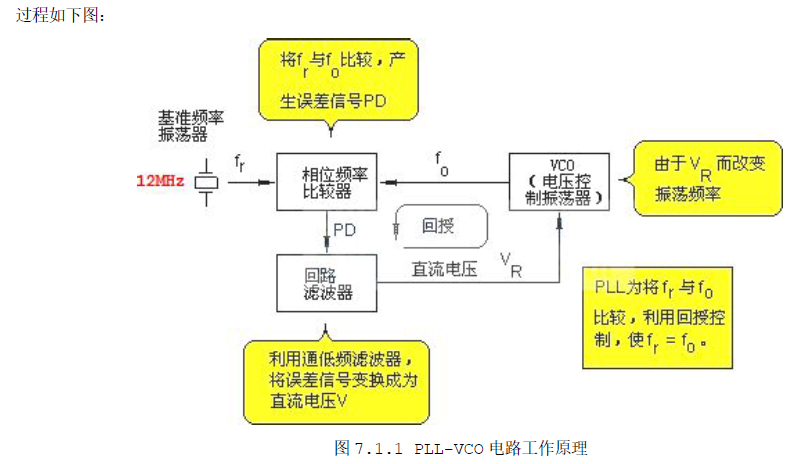

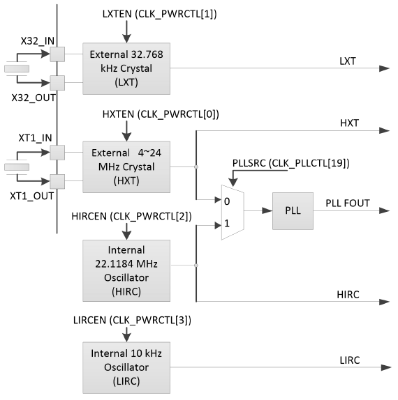


时钟控制器为整个芯片提供时钟源,包括系统时钟和所有外围设备时钟。该控制器还通过单独时钟的开或关,时钟源选择和分频器来进行功耗控制。在CPU使能低功耗PDEN(CLK_PWRCTL[7]) 位和Cortex®-M4内核执行WFI指令后,芯片才能进入低功耗模式。直到唤醒中断发生,芯片才会退出低功耗模式。在低功耗模式下,时钟控制器会关闭外部4~24MHz高速晶振和内部22.1184MHz高速RC振荡器,以降低整个系统功耗。下图所示各模块时钟发生器和时钟源的简图。
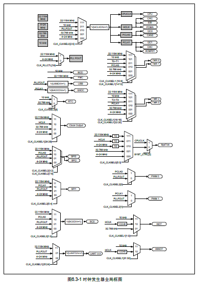
时钟发生器
时钟发生器由如下5个时钟源组成:
外部32.768 kHz低速晶振(LXT)
外部4~24 MHz高速晶振(HXT)
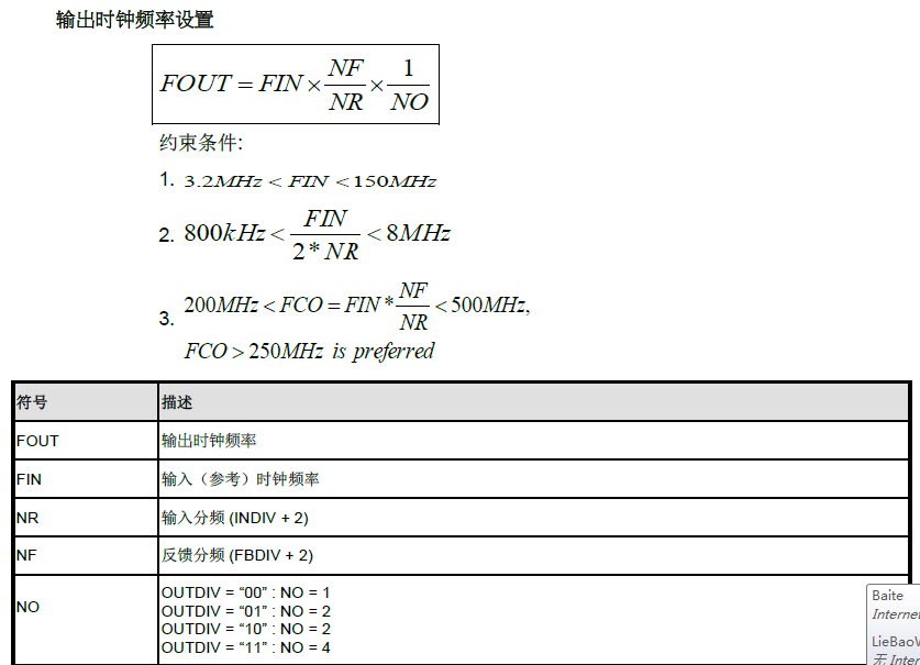
可编程的PLL输出时钟频率(PLLFOUT),PLL 由外部 4~24 MHz 晶振或内部 22.1184
MHz 振荡器提供时钟源)
内部22.1184 MHz高速振荡器(HIRC)
内部10 kHz低速RC振荡器(LIRC)

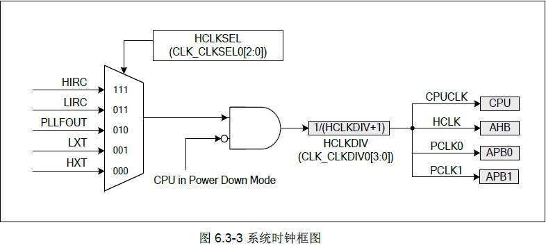
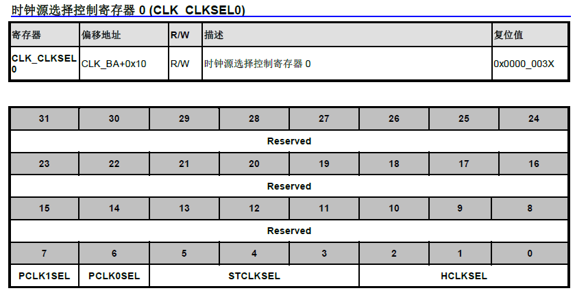
系统时钟有 5 个可选时钟源,由时钟发生器产生。时钟源切换取决于寄存器HCLKSEL
(CLK_CLKSEL0[2:0]). 其框图如下所示。
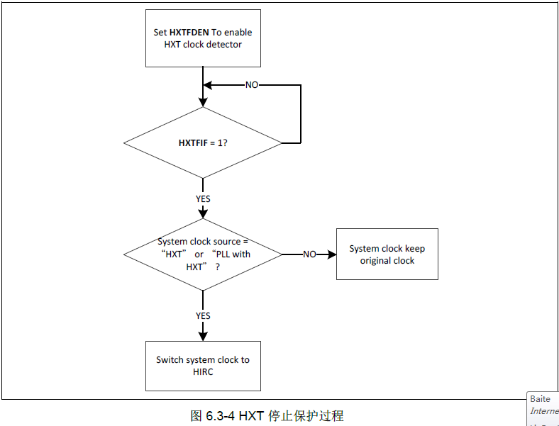
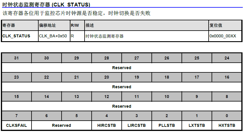
有两个时钟失败检测器来观察HXT和LXT时钟源的状况,而且都有独立的使能和中断控制设置。当
HXT检测器使能时,HIRC时钟也自动使能。当LXT检测器使能时,LIRC时钟也自动使能。
当HXT时钟检测器使能,如果检测到HXT时钟停止且满足下面条件:系统的时钟源来自HXT或者系
统时钟源来自PLL(PLL的输入时钟为HXT),系统时钟将自动切换到HIRC。如果HXT时钟停止条件
检测到,HXTFIF (CLK_CLKDSTS[0])将被设置为1,此时如果HXTFIE (CLK_CLKDCTL[5])有置
位,芯片将进入中断。用户可以试着去恢复HXT,通过禁止HXT和重新使能HXT来确认时钟稳定标
志位是否已设置为1。如果HXT时钟稳定标志位有设置为1,这就意味着HXT在重新使能后已恢复震
荡,此时用户可以重新把系统时钟切换到HXT了。
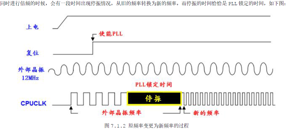
HXT时钟停止检测和系统时钟切换到HIRC的过程如下图所示:
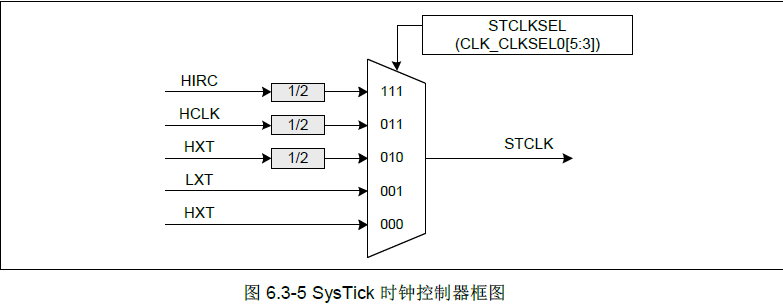
Cortex® -M4内核的SysTick 时钟源可以选择CPU时钟或外部时钟(SYST_CTRL[2]) 。如果使用外部
时钟,SysTick 时钟 (STCLK) 有 5 个可选时钟源.时钟源切换取决于寄存器STCLKSEL
(CLK_CLKSEL0[5:3])。其框图如下所示:
外设时钟
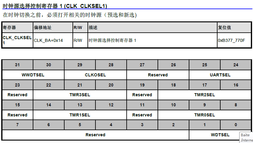
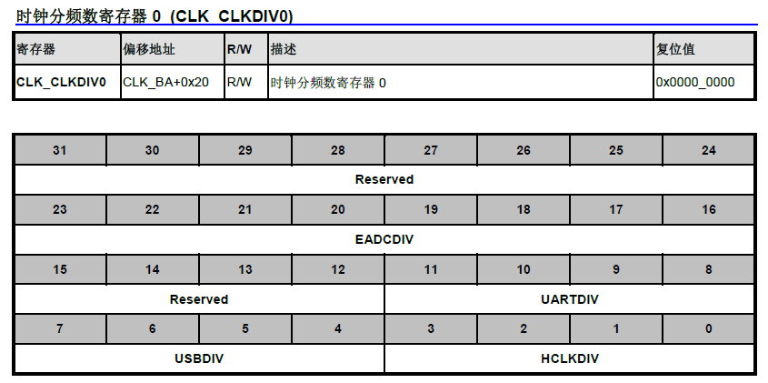
外设时钟可以有不同的时钟源做切换设置。主要取决于不同的外设。请参看寄存器CLK_CLKSEL1
和 CLK_CLKSEL2。 在5.3.8章节有详细描述。
掉电模式时钟
当芯片进入掉电模式,系统时钟和一些时钟源以及一些外设时钟将被关闭。也有一些时钟源与外设
时钟仍在工作。
如下时钟仍在工作:
时钟发生器
10 kHz内部低速RC振荡器
32.768 kHz外部低速晶振时钟
外设时钟 (当模块的时钟源来自32.768 kHz外部低速晶振时钟或10 kHz内部低速RC振荡器)
时钟输出
该设备带有一个2的若干次幂的频率分频器,该分频器由16个链式的二分频器组成的移位寄存器。
其中哪一级的值被输出,由一个16选1的多路转换器选择,该多路转换器接到CLKO管脚上。因此共
有2的16种次幂的时钟分频选择,分频范围从Fin/21 到 Fin/216,此处Fin是到时钟分频器的时钟输入
频率。
输出公式:Fout = Fin/2(N+1), 其中 Fin 为输入时钟频率,Fout为时钟分频器输出频率,N 为FREQSEL
(CLK_CLKOCTL[3:0])中的4位值。
往CLKOEN (CLK_CLKOCTL[4])写1,分级计数器开始计数。往CLKOEN (CLK_CLKOCTL[4])写
0,分级计数器持续计数,直到分频时钟达到低电平并会保持在低电平状态。

- void CLK_DisablePLL(void)
- {
- CLK->PLLCON |= CLK_PLLCON_PD_Msk;
- }
- #define CLK_PLLCON_PD_Pos 16 /*!< CLK_T::PLLCON: PD Position */
- #define CLK_PLLCON_PD_Msk (1ul << CLK_PLLCON_PD_Pos) /*!< CLK_T::PLLCON: PD Mask */
- typedef struct
- {
- /**
- * @var CLK_T::PWRCON
- * Offset: 0x00 System Power-down Control Register
- * ---------------------------------------------------------------------------------------------------
- * |Bits |Field |Descriptions
- * | :----: | :----: | :---- |
- * |[0] |XTL12M_EN |External 4~24 MHz High Speed Crystal Enable (HXT) Control (Write Protect)
- * | | |The bit default value is set by flash controller user configuration register CFOSC (Config0[26:24]).
- * | | |When the default clock source is from external 4~24 MHz high speed crystal, this bit is set to 1 automatically.
- * | | |0 = External 4~24 MHz high speed crystal oscillator (HXT) Disabled.
- * | | |1 = External 4~24 MHz high speed crystal oscillator (HXT) Enabled.
- * | | |Note: This bit is write protected bit. Refer to the REGWRPROT register.
- * |[2] |OSC22M_EN |Internal 22.1184 MHz High Speed Oscillator (HIRC) Enable Control (Write Protect)
- * | | |0 = Internal 22.1184 MHz high speed oscillator (HIRC) Disabled.
- * | | |1 = Internal 22.1184 MHz high speed oscillator (HIRC) Enabled.
- * | | |Note: This bit is write protected bit. Refer to the REGWRPROT register.
- * |[3] |OSC10K_EN |Internal 10 KHz Low Speed Oscillator (LIRC) Enable Control (Write Protect)
- * | | |0 = Internal 10 kHz low speed oscillator (LIRC) Disabled.
- * | | |1 = Internal 10 kHz low speed oscillator (LIRC) Enabled.
- * | | |Note: This bit is write protected bit. Refer to the REGWRPROT register.
- * |[4] |PD_WU_DLY |Wake-up Delay Counter Enable Control (Write Protect)
- * | | |When the chip wakes up from Power-down mode, the clock control will delay certain clock cycles to wait system clock stable.
- * | | |The delayed clock cycle is 4096 clock cycles when chip work at external 4~24 MHz high speed crystal, and 256 clock cycles when chip work at internal 22.1184 MHz high speed oscillator.
- * | | |0 = Clock cycles delay Disabled.
- * | | |1 = Clock cycles delay Enabled.
- * | | |Note: This bit is write protected bit. Refer to the REGWRPROT register.
- * |[5] |PD_WU_INT_EN|Power-Down Mode Wake-Up Interrupt Enable Control (Write Protect)
- * | | |0 = Power-down mode wake-up interrupt Disabled.
- * | | |1 = Power-down mode wake-up interrupt Enabled.
- * | | |Note1: The interrupt will occur when both PD_WU_STS and PD_WU_INT_EN are high.
- * | | |Note2: This bit is write protected bit. Refer to the REGWRPROT register.
- * |[6] |PD_WU_STS |Power-down Mode Wake-Up Interrupt Status
- * | | |Set by "Power-down wake-up event", it indicates that resume from Power-down mode.
- * | | |The flag is set if the GPIO, USB, UART, WDT, TIMER, I2C or BOD wake-up occurred.
- * | | |This bit can be cleared to 0 by software writing "1".
- * | | |Note: This bit is working only if PD_WU_INT_EN (PWRCON[5]) set to 1.
- * |[7] |PWR_DOWN_EN|System Power-down Enable Bit (Write Protect)
- * | | |When this bit is set to 1, Power-down mode is enabled and chip Power-down behavior will depends on the PD_WAIT_CPU bit
- * | | |(a) If the PD_WAIT_CPU is 0, then the chip enters Power-down mode immediately after the PWR_DOWN_EN bit set.
- * | | |(b) if the PD_WAIT_CPU is 1, then the chip keeps active till the CPU sleep mode is also active and then the chip enters Power-down mode (recommend)
- * | | |When chip wakes up from Power-down mode, this bit is cleared by hardware.
- * | | |User needs to set this bit again for next Power-down.
- * | | |In Power-down mode, 4~24 MHz external high speed crystal oscillator (HXT) and the 22.1184 MHz internal high speed RC oscillator (HIRC) will be disabled in this mode, but the 10 kHz internal low speed RC oscillator (LIRC) is not controlled by Power-down mode.
- * | | |In Power- down mode, the PLL and system clock are disabled, and ignored the clock source selection. The clocks of peripheral are not controlled by Power-down mode, if the peripheral clock source is from the 10 kHz internal low speed RC oscillator (LIRC).
- * | | |The clocks of peripheral are not controlled by Power-down mode, if the peripheral clock source is from the internal 10 kHz low speed oscillator.
- * | | |0 = Chip operating normally or chip in Idle mode because of WFI command.
- * | | |1 = Chip enters Power-down mode instantly or waits CPU sleep command WFI.
- * | | |Note: This bit is write protected bit. Refer to the REGWRPROT register.
- * |[8] |PD_WAIT_CPU|This Bit Control The Power-Down Entry Condition (Write Protect)
- * | | |0 = Chip enters Power-down mode when the PWR_DOWN_EN bit is set to 1.
- * | | |1 = Chip enters Power-down mode when the both PD_WAIT_CPU and PWR_DOWN_EN bits are set to 1 and CPU run WFI instruction.
- * | | |Note: This bit is write protected bit. Refer to the REGWRPROT register.
- * @var CLK_T::AHBCLK
- * Offset: 0x04 AHB Devices Clock Enable Control Register
- * ---------------------------------------------------------------------------------------------------
- * |Bits |Field |Descriptions
- * | :----: | :----: | :---- |
- * |[1] |PDMA_EN |PDMA Controller Clock Enable Control
- * | | |0 = PDMA peripheral clock Disabled.
- * | | |1 = PDMA peripheral clock Enabled.
- * |[2] |ISP_EN |Flash ISP Controller Clock Enable Control
- * | | |0 = Flash ISP peripheral clock Disabled.
- * | | |1 = Flash ISP peripheral clock Enabled.
- * @var CLK_T::APBCLK
- * Offset: 0x08 APB Devices Clock Enable Control Register
- * ---------------------------------------------------------------------------------------------------
- * |Bits |Field |Descriptions
- * | :----: | :----: | :---- |
- * |[0] |WDT_EN |Watchdog Timer Clock Enable Control (Write Protect)
- * | | |0 = Watchdog Timer clock Disabled.
- * | | |1 = Watchdog Timer clock Enabled.
- * | | |Note: This bit is write protected bit. Refer to the REGWRPROT register.
- * |[2] |TMR0_EN |Timer0 Clock Enable Control
- * | | |0 = Timer0 clock Disabled.
- * | | |1 = Timer0 clock Enabled.
- * |[3] |TMR1_EN |Timer1 Clock Enable Control
- * | | |0 = Timer1 clock Disabled.
- * | | |1 = Timer1 clock Enabled.
- * |[4] |TMR2_EN |Timer2 Clock Enable Control
- * | | |0 = Timer2 clock Disabled.
- * | | |1 = Timer2 clock Enabled.
- * |[5] |TMR3_EN |Timer3 Clock Enable Control
- * | | |0 = Timer3 clock Disabled.
- * | | |1 = Timer3 clock Enabled.
- * |[6] |FDIV_EN |Frequency Divider Output Clock Enable Control
- * | | |0 = FDIV clock Disabled.
- * | | |1 = FDIV clock Enabled.
- * |[8] |I2C0_EN |I2C0 Clock Enable Control
- * | | |0 = I2C0 clock Disabled.
- * | | |1 = I2C0 clock Enabled.
- * |[9] |I2C1_EN |I2C1 Clock Enable Control
- * | | |0 = I2C1 clock Disabled.
- * | | |1 = I2C1 clock Enabled.
- * |[12] |SPI0_EN |SPI0 Clock Enable Control
- * | | |0 = SPI0 clock Disabled.
- * | | |1 = SPI0 clock Enabled.
- * |[13] |SPI1_EN |SPI1 Clock Enable Control
- * | | |0 = SPI1 clock Disabled.
- * | | |1 = SPI1 clock Enabled.
- * |[14] |SPI2_EN |SPI2 Clock Enable Control
- * | | |0 = SPI2 clock Disabled.
- * | | |1 = SPI2 clock Enabled.
- * |[16] |UART0_EN |UART0 Clock Enable Control
- * | | |0 = UART0 clock Disabled.
- * | | |1 = UART0 clock Enabled.
- * |[17] |UART1_EN |UART1 Clock Enable Control
- * | | |0 = UART1 clock Disabled.
- * | | |1 = UART1 clock Enabled.
- * |[20] |PWM01_EN |PWM_01 Clock Enable Control
- * | | |0 = PWM01 clock Disabled.
- * | | |1 = PWM01 clock Enabled.
- * |[21] |PWM23_EN |PWM_23 Clock Enable Control
- * | | |0 = PWM23 clock Disabled.
- * | | |1 = PWM23 clock Enabled.
- * |[27] |USBD_EN |USB 2.0 FS Device Controller Clock Enable Control
- * | | |0 = USB clock Disabled.
- * | | |1 = USB clock Enabled.
- * |[28] |ADC_EN |Analog-Digital-Converter (ADC) Clock Enable Control
- * | | |0 = ADC clock Disabled.
- * | | |1 = ADC clock Enabled.
- * |[29] |I2S_EN |I2S Clock Enable Control
- * | | |0 = I2S clock Disabled.
- * | | |1 = I2S clock Enabled.
- * |[31] |PS2_EN |PS/2 Clock Enable Control
- * | | |0 = PS/2 clock Disabled.
- * | | |1 = PS/2 clock Enabled.
- * @var CLK_T::CLKSTATUS
- * Offset: 0x0C Clock status monitor Register
- * ---------------------------------------------------------------------------------------------------
- * |Bits |Field |Descriptions
- * | :----: | :----: | :---- |
- * |[0] |XTL12M_STB|External 4~24 MHz High Speed Crystal (HXT) Clock Source Stable Flag (Read Only)
- * | | |0 = External 4~24 MHz high speed crystal clock (HXT) is not stable or disabled.
- * | | |1 = External 4~24 MHz high speed crystal clock (HXT) is stable and enabled.
- * |[2] |PLL_STB |Internal PLL Clock Source Stable Flag (Read Only)
- * | | |0 = Internal PLL clock is not stable or disabled.
- * | | |1 = Internal PLL clock is stable in normal mode.
- * |[3] |OSC10K_STB|Internal 10 KHz Low Speed Oscillator (LIRC) Clock Source Stable Flag (Read Only)
- * | | |0 = Internal 10 kHz low speed oscillator clock (LIRC) is not stable or disabled.
- * | | |1 = Internal 10 kHz low speed oscillator clock (LIRC) is stable and enabled.
- * |[4] |OSC22M_STB|Internal 22.1184 MHz High Speed Oscillator (HIRC) Clock Source Stable Flag (Read Only)
- * | | |0 = Internal 22.1184 MHz high speed oscillator (HIRC) clock is not stable or disabled.
- * | | |1 = Internal 22.1184 MHz high speed oscillator (HIRC) clock is stable and enabled.
- * |[7] |CLK_SW_FAIL|Clock Switching Fail Flag
- * | | |This bit is updated when software switches system clock source.
- * | | |If switch target clock is stable, this bit will be set to 0.
- * | | |If switch target clock is not stable, this bit will be set to 1.
- * | | |0 = Clock switching success.
- * | | |1 = Clock switching failure.
- * | | |Note1: On NUC123xxxANx, this bit can be cleared to 0 by software writing "1".
- * | | |Note2: On NUC123xxxAEx, this bit is read only. After selected clock source is stable, hardware will switch system clock to selected clock automatically, and CLK_SW_FAIL will be cleared automatically by hardware.
- * @var CLK_T::CLKSEL0
- * Offset: 0x10 Clock Source Select Control Register 0
- * ---------------------------------------------------------------------------------------------------
- * |Bits |Field |Descriptions
- * | :----: | :----: | :---- |
- * |[2:0] |HCLK_S |HCLK Clock Source Select (Write Protect)
- * | | |The 3-bit default value is reloaded from the value of CFOSC (CONFIG0[26:24]) in user configuration register of Flash controller by any reset.
- * | | |Therefore the default value is either 000b or 111b.
- * | | |000 = Clock source from external 4~24 MHz high speed crystal oscillator clock.
- * | | |001 = Clock source from PLL/2 clock.
- * | | |010 = Clock source from PLL clock.
- * | | |011 = Clock source from internal 10 kHz low speed oscillator clock.
- * | | |111 = Clock source from internal 22.1184 MHz high speed oscillator clock.
- * | | |Note1: Before clock switching, the related clock sources (both pre-select and new-select) must be turn on.
- * | | |Note2: These bits are write protected bit. Refer to the REGWRPROT register.
- * |[5:3] |STCLK_S |Cortex-M0 SysTick Clock Source Select (Write Protect)
- * | | |If SYST_CSR[2] = 1, SysTick clock source is from HCLK.
- * | | |If SYST_CSR[2] = 0, SysTick clock source is defined by STCLK_S(CLKSEL0[5:3]).
- * | | |000 = Clock source from external 4~24 MHz high speed crystal clock.
- * | | |010 = Clock source from external 4~24 MHz high speed crystal clock/2.
- * | | |011 = Clock source from HCLK/2.
- * | | |111 = Clock source from internal 22.1184 MHz high speed oscillator clock/2.
- * | | |Note1: If SysTick clock source is not from HCLK (i.e. SYST_CSR[2] = 0), SysTick clock source must less than or equal to HCLK/2.
- * | | |Note2: These bits are write protected bit. Refer to the REGWRPROT register.
- * @var CLK_T::CLKSEL1
- * Offset: 0x14 Clock Source Select Control Register 1
- * ---------------------------------------------------------------------------------------------------
- * |Bits |Field |Descriptions
- * | :----: | :----: | :---- |
- * |[1:0] |WDT_S |Watchdog Timer Clock Source Select (Write Protect)
- * | | |10 = Clock source from HCLK/2048 clock.
- * | | |11 = Clock source from internal 10 kHz low speed oscillator clock.
- * | | |Note: These bits are write protected bit. Refer to the REGWRPROT register.
- * |[3:2] |ADC_S |ADC Clock Source Select
- * | | |00 = Clock source from external 4~24 MHz high speed crystal oscillator clock.
- * | | |01 = Clock source from PLL clock.
- * | | |10 = Clock source from HCLK.
- * | | |11 = Clock source from internal 22.1184 MHz high speed oscillator clock.
- * |[4] |SPI0_S |SPI0 Clock Source Selection
- * | | |0 = Clock source from PLL clock.
- * | | |1 = Clock source from HCLK.
- * |[5] |SPI1_S |SPI1 Clock Source Selection
- * | | |0 = Clock source from PLL clock.
- * | | |1 = Clock source from HCLK.
- * |[6] |SPI2_S |SPI2 Clock Source Selection
- * | | |0 = Clock source from PLL clock.
- * | | |1 = Clock source from HCLK.
- * |[10:8] |TMR0_S |TIMER0 Clock Source Selection
- * | | |000 = Clock source from external 4~24 MHz high speed crystal clock.
- * | | |010 = Clock source from HCLK.
- * | | |011 = Clock source from external trigger.
- * | | |101 = Clock source from internal 10 kHz low speed oscillator clock.
- * | | |111 = Clock source from internal 22.1184 MHz high speed oscillator clock.
- * | | |Others = Reserved.
- * |[14:12] |TMR1_S |TIMER1 Clock Source Selection
- * | | |000 = Clock source from external 4~24 MHz high speed crystal clock.
- * | | |010 = Clock source from HCLK.
- * | | |011 = Clock source from external trigger.
- * | | |101 = Clock source from internal 10 kHz low speed oscillator clock.
- * | | |111 = Clock source from internal 22.1184 MHz high speed oscillator clock.
- * | | |Others = Reserved.
- * |[18:16] |TMR2_S |TIMER2 Clock Source Selection
- * | | |000 = Clock source from external 4~24 MHz high speed crystal clock.
- * | | |010 = Clock source from HCLK.
- * | | |011 = Clock source from external trigger.
- * | | |101 = Clock source from internal 10 kHz low speed oscillator clock.
- * | | |111 = Clock source from internal 22.1184 MHz high speed oscillator clock.
- * | | |Others = Reserved.
- * |[22:20] |TMR3_S |TIMER3 Clock Source Selection
- * | | |000 = Clock source from external 4~24 MHz high speed crystal clock.
- * | | |010 = Clock source from HCLK.
- * | | |011 = Reserved.
- * | | |101 = Clock source from internal 10 kHz low speed oscillator clock.
- * | | |111 = Clock source from internal 22.1184 MHz high speed oscillator clock.
- * | | |Others = Reserved.
- * |[25:24] |UART_S |UART Clock Source Selection
- * | | |00 = Clock source from external 4~24 MHz high speed crystal oscillator clock.
- * | | |01 = Clock source from PLL clock.
- * | | |11 = Clock source from internal 22.1184 MHz high speed oscillator clock.
- * |[29:28] |PWM01_S |PWM0 and PWM1 Clock Source Selection
- * | | |PWM0 and PWM1 used the same clock source; both of them used the same prescaler.
- * | | |The clock source of PWM0 and PWM1 is defined by PWM01_S (CLKSEL1[29:28]) and PWM01_S_E (CLKSEL2[8]).
- * | | |If PWM01_S_E = 0, the clock source of PWM0 and PWM1 defined by PWM01_S list below:
- * | | |00 = Clock source from external 4~24 MHz high speed crystal oscillator clock.
- * | | |10 = Clock source from HCLK.
- * | | |11 = Clock source from internal 22.1184 MHz high speed oscillator clock.
- * | | |If PWM01_S_E = 1, the clock source of PWM0 and PWM1 defined by PWM01_S list below:
- * | | |00 = Reserved.
- * | | |01 = Reserved.
- * | | |10 = Reserved.
- * | | |11 = Clock source from internal 10 kHz low speed oscillator clock.
- * |[31:30] |PWM23_S |PWM2 and PWM3 Clock Source Selection
- * | | |PWM2 and PWM3 used the same clock source; both of them used the same prescaler.
- * | | |The clock source of PWM2 and PWM3 is defined by PWM23_S (CLKSEL1[31:30]) and PWM23_S_E (CLKSEL2[9]).
- * | | |If PWM23_S_E = 0, theclock source of PWM2 and PWM3 defined by PWM23_S list below:
- * | | |00 = Clock source from external 4~24 MHz high speed crystal oscillator clock.
- * | | |10 = Clock source from HCLK.
- * | | |11 = Clock source from internal 22.1184 MHz high speed oscillator clock.
- * | | |If PWM23_S_E = 1, the clock source of PWM2 and PWM3 defined by PWM23_S list below:
- * | | |00 = Reserved.
- * | | |01 = Reserved.
- * | | |10 = Reserved.
- * | | |11 = Clock source from internal 10 kHz low speed oscillator clock.
- * @var CLK_T::CLKDIV
- * Offset: 0x18 Clock Divider Number Register
- * ---------------------------------------------------------------------------------------------------
- * |Bits |Field |Descriptions
- * | :----: | :----: | :---- |
- * |[3:0] |HCLK_N |HCLK Clock Divide Number From HCLK Clock Source
- * | | |HCLK clock frequency = (HCLK clock source frequency) / (HCLK_N + 1).
- * |[7:4] |USB_N |USB Clock Divide Number From PLL Clock
- * | | |USB clock frequency = (PLL frequency) / (USB_N + 1).
- * |[11:8] |UART_N |UART Clock Divide Number From UART Clock Source
- * | | |UART clock frequency = (UART clock source frequency) / (UART_N + 1).
- * |[23:16] |ADC_N |ADC Clock Divide Number From ADC Clock Source
- * | | |ADC clock frequency = (ADC clock source frequency) / (ADC_N + 1).
- * @var CLK_T::CLKSEL2
- * Offset: 0x1C Clock Source Select Control Register 2
- * ---------------------------------------------------------------------------------------------------
- * |Bits |Field |Descriptions
- * | :----: | :----: | :---- |
- * |[1:0] |I2S_S |I2S Clock Source Selection
- * | | |00 = Clock source from external 4~24 MHz high speed crystal oscillator clock.
- * | | |01 = Clock source from PLL clock.
- * | | |10 = Clock source from HCLK.
- * | | |11 = Clock source from internal 22.1184 MHz high speed oscillator clock.
- * |[3:2] |FRQDIV_S |Clock Divider Clock Source Selection
- * | | |00 = Clock source from external 4~24 MHz high speed crystal oscillator clock.
- * | | |10 = Clock source from HCLK.
- * | | |11 = Clock source from internal 22.1184 MHz high speed oscillator clock.
- * |[8] |PWM01_S_E |PWM0 and PWM1 Clock Source Selection Extend
- * | | |PWM0 and PWM1 used the same clock source; both of them used the same prescaler.
- * | | |The clock source of PWM0 and PWM1 is defined by PWM01_S (CLKSEL1[29:28]) and PWM01_S_E (CLKSEL2[8]).
- * | | |If PWM01_S_E = 0, the clock source of PWM0 and PWM1 defined by PWM01_S list below:
- * | | |00 = Clock source from external 4~24 MHz high speed crystal oscillator clock.
- * | | |10 = Clock source from HCLK.
- * | | |11 = Clock source from internal 22.1184 MHz high speed oscillator clock.
- * | | |If PWM01_S_E = 1, the clock source of PWM0 and PWM1 defined by PWM01_S list below:
- * | | |00 = Reserved.
- * | | |01 = Reserved.
- * | | |10 = Reserved.
- * | | |11 = Clock source from internal 10 kHz low speed oscillator clock.
- * |[9] |PWM23_S_E |PWM2 and PWM3 Clock Source Selection Extend
- * | | |PWM2 and PWM3 used the same clock source; both of them used the same prescaler.
- * | | |The clock source of PWM2 and PWM3 is defined by PWM23_S (CLKSEL1[31:30]) and PWM23_S_E (CLKSEL2[9]).
- * | | |If PWM23_S_E = 0, the clock source of PWM2 and PWM3 defined by PWM23_S list below:
- * | | |00 = Clock source from external 4~24 MHz high speed crystal oscillator clock.
- * | | |10 = Clock source from HCLK.
- * | | |11 = Clock source from internal 22.1184 MHz high speed oscillator clock.
- * | | |If PWM23_S_E = 1, the clock source of PWM2 and PWM3 defined by PWM23_S list below:
- * | | |00 = Reserved.
- * | | |01 = Reserved.
- * | | |10 = Reserved.
- * | | |11 = Clock source from internal 10 kHz low speed oscillator clock.
- * |[17:16] |WWDT_S |Window Watchdog Timer Clock Source Selection
- * | | |10 = Clock source from HCLK/2048 clock.
- * | | |11 = Clock source from internal 10 kHz low speed oscillator clock.
- * @var CLK_T::PLLCON
- * Offset: 0x20 PLL Control Register
- * ---------------------------------------------------------------------------------------------------
- * |Bits |Field |Descriptions
- * | :----: | :----: | :---- |
- * |[8:0] |FB_DV |PLL Feedback Divider Control Bits
- * | | |Refer to the PLL formulas.
- * |[13:9] |IN_DV |PLL Input Divider Control Bits
- * | | |Refer to the PLL formulas.
- * |[15:14] |OUT_DV |PLL Output Divider Control Bits
- * | | |Refer to the PLL formulas.
- * |[16] |PD |Power-down Mode
- * | | |If the PWR_DOWN_EN bit is set to 1 in PWRCON register, the PLL will enter Power-down mode too.
- * | | |0 = PLL is in Normal mode.
- * | | |1 = PLL is in Power-down mode (default).
- * |[17] |BP |PLL Bypass Control
- * | | |0 = PLL is in Normal mode (default).
- * | | |1 = PLL clock output is same as PLL source clock input.
- * |[18] |OE |PLL OE (FOUT Enable) Control
- * | | |0 = PLL FOUT Enabled.
- * | | |1 = PLL FOUT is fixed low.
- * |[19] |PLL_SRC |PLL Source Clock Selection
- * | | |0 = PLL source clock from external 4~24 MHz high speed crystal.
- * | | |1 = PLL source clock from internal 22.1184 MHz high speed oscillator.
- * @var CLK_T::FRQDIV
- * Offset: 0x24 Frequency Divider Control Register
- * ---------------------------------------------------------------------------------------------------
- * |Bits |Field |Descriptions
- * | :----: | :----: | :---- |
- * |[3:0] |FSEL |Divider Output Frequency Selection Bits
- * | | |The formula of output frequency is Fout = Fin/2(N+1).
- * | | |Fin is the input clock frequency.
- * | | |Fout is the frequency of divider output clock.
- * | | |N is the 4-bit value of FSEL[3:0].
- * |[4] |DIVIDER_EN|Frequency Divider Enable Bit
- * | | |0 = Frequency Divider function Disabled.
- * | | |1 = Frequency Divider function Enabled.
- * @var CLK_T::APBDIV
- * Offset: 0x2C APB Divider Control Register
- * ---------------------------------------------------------------------------------------------------
- * |Bits |Field |Descriptions
- * | :----: | :----: | :---- |
- * |[0] |APBDIV |APB Divider Enable Bit
- * | | |0 = PCLK is HCLK.
- * | | |1 = PCLK is HCLK/2.
- */
- __IO uint32_t PWRCON; /* Offset: 0x00 System Power-down Control Register */
- __IO uint32_t AHBCLK; /* Offset: 0x04 AHB Devices Clock Enable Control Register */
- __IO uint32_t APBCLK; /* Offset: 0x08 APB Devices Clock Enable Control Register */
- __IO uint32_t CLKSTATUS; /* Offset: 0x0C Clock status monitor Register */
- __IO uint32_t CLKSEL0; /* Offset: 0x10 Clock Source Select Control Register 0 */
- __IO uint32_t CLKSEL1; /* Offset: 0x14 Clock Source Select Control Register 1 */
- __IO uint32_t CLKDIV; /* Offset: 0x18 Clock Divider Number Register */
- __IO uint32_t CLKSEL2; /* Offset: 0x1C Clock Source Select Control Register 2 */
- __IO uint32_t PLLCON; /* Offset: 0x20 PLL Control Register */
- __IO uint32_t FRQDIV; /* Offset: 0x24 Frequency Divider Control Register */
- __I uint32_t RESERVE0;
- __IO uint32_t APBDIV; /* Offset: 0x2C APB Divider Control Register */
- } CLK_T;
- #define CLK ((CLK_T *) CLK_BASE) /*!< System Clock Controller Configuration Struct */void CLK_SetHCLK(uint32_t u32ClkSrc, uint32_t u32ClkDiv)
- {
- uint32_t u32HIRCSTB;
- /* Read HIRC clock source stable flag */
- u32HIRCSTB = CLK->CLKSTATUS & CLK_CLKSTATUS_OSC22M_STB_Msk;
- /* Switch to HIRC for Safe. Avoid HCLK too high when applying new divider. */
- CLK->PWRCON |= CLK_CLKSTATUS_OSC22M_STB_Msk;
- CLK_WaitClockReady(CLK_CLKSTATUS_OSC22M_STB_Msk);
- CLK->CLKSEL0 = (CLK->CLKSEL0 & (~CLK_CLKSEL0_HCLK_S_Msk)) | CLK_CLKSEL0_HCLK_S_HIRC;
- /* Apply new Divider */
- CLK->CLKDIV = (CLK->CLKDIV & (~CLK_CLKDIV_HCLK_N_Msk)) | u32ClkDiv;
- /* Switch HCLK to new HCLK source */
- CLK->CLKSEL0 = (CLK->CLKSEL0 & (~CLK_CLKSEL0_HCLK_S_Msk)) | u32ClkSrc;
- /* Update System Core Clock */
- SystemCoreClockUpdate();
- /* Disable HIRC if HIRC is disabled before switching HCLK source */
- if( u32HIRCSTB == )
- CLK->PWRCON &= ~CLK_CLKSTATUS_OSC22M_STB_Msk;
- }
- /* Switch HCLK clock source to HXT and HCLK source divide 1 */
- CLK_SetHCLK(CLK_CLKSEL0_HCLK_S_HXT, CLK_CLKDIV_HCLK());
- /* Set PLL to power down mode and PLL_STB bit in CLKSTATUS register will be cleared by hardware. */
- CLK_DisablePLL();
- /* Set PLL frequency */
- CLK->PLLCON = g_au32PllSetting[i];
- /* Waiting for PLL clock ready */
- CLK_WaitClockReady(CLK_CLKSTATUS_PLL_STB_Msk);
- /* Switch HCLK clock source to PLL */
- CLK_SetHCLK(CLK_CLKSEL0_HCLK_S_PLL, CLK_CLKDIV_HCLK());
- printf(" Change system clock to %d Hz ...................... ", SystemCoreClock);
- /* Output selected clock to CKO, CKO Clock = HCLK / 2^(1 + 1) */
- CLK_EnableCKO(CLK_CLKSEL2_FRQDIV_S_HCLK, , );
- void CLK_EnableCKO(uint32_t u32ClkSrc, uint32_t u32ClkDiv, uint32_t u32ClkDivBy1En)
- {
- /* CKO = clock source / 2^(u32ClkDiv + 1) */
- CLK->FRQDIV = (CLK_FRQDIV_DIVIDER_EN_Msk | u32ClkDiv) ;
- /* Enable CKO clock source */
- CLK_EnableModuleClock(FDIV_MODULE);
- /* Select CKO clock source */
- CLK_SetModuleClock(FDIV_MODULE, u32ClkSrc, );
- }
- uint32_t g_au32PllSetting[] =
- {
- CLK_PLLCON_PLL_SRC_HXT | CLK_PLLCON_NR() | CLK_PLLCON_NF() | CLK_PLLCON_NO_4, /* PLL = 25MHz */
- CLK_PLLCON_PLL_SRC_HXT | CLK_PLLCON_NR() | CLK_PLLCON_NF() | CLK_PLLCON_NO_4, /* PLL = 29MHz */
- CLK_PLLCON_PLL_SRC_HXT | CLK_PLLCON_NR() | CLK_PLLCON_NF() | CLK_PLLCON_NO_4, /* PLL = 33MHz */
- CLK_PLLCON_PLL_SRC_HXT | CLK_PLLCON_NR() | CLK_PLLCON_NF() | CLK_PLLCON_NO_4, /* PLL = 37MHz */
- CLK_PLLCON_PLL_SRC_HXT | CLK_PLLCON_NR() | CLK_PLLCON_NF() | CLK_PLLCON_NO_4, /* PLL = 41MHz */
- CLK_PLLCON_PLL_SRC_HXT | CLK_PLLCON_NR() | CLK_PLLCON_NF() | CLK_PLLCON_NO_4, /* PLL = 45MHz */
- CLK_PLLCON_PLL_SRC_HXT | CLK_PLLCON_NR() | CLK_PLLCON_NF() | CLK_PLLCON_NO_4 /* PLL = 49MHz */
- };
- #define CLK_PLLCON_PLL_SRC_HXT 0x00000000UL /*!< For PLL clock source is HXT. 4MHz < FIN < 24MHz */
- #define CLK_PLLCON_PLL_SRC_HIRC 0x00080000UL /*!< For PLL clock source is HIRC.4MHz < FIN < 24MHz */
- #define CLK_PLLCON_NR(x) (((x)-2)<<9) /*!< x must be constant and 2 <= x <= 33. 1.6MHz < FIN/NR < 15MHz */
- #define CLK_PLLCON_NF(x) ((x)-2) /*!< x must be constant and 2 <= x <= 513. 100MHz < FIN*NF/NR < 200MHz. (120MHz < FIN*NF/NR < 200MHz is preferred.) */
- #define CLK_PLLCON_NO_1 0x0000UL /*!< For output divider is 1 */
- #define CLK_PLLCON_NO_2 0x4000UL /*!< For output divider is 2 */
- #define CLK_PLLCON_NO_4 0xC000UL /*!< For output divider is 4 */
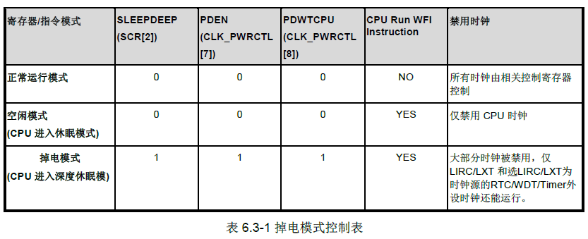
当芯片进入掉电模式时,用户可以通过一些中断源唤醒芯片。用户必须在设置PDEN 位 (CLK_PWRCTL[7] ) 之前,使能相关的中断源及相应的NVIC IRQ 使能位 (NVIC_ISER) 从而保证芯片能进入掉电模式以及能够成功被唤醒。


- void SYS_Init(void)
- {
- /*---------------------------------------------------------------------------------------------------------*/
- /* Init System Clock */
- /*---------------------------------------------------------------------------------------------------------*/
- /* Enable HIRC clock (Internal RC 22.1184MHz) */
- CLK->PWRCTL |= CLK_PWRCTL_HIRCEN_Msk;
- /* Wait for HIRC clock ready */
- while(!(CLK->STATUS & CLK_STATUS_HIRCSTB_Msk));
- /* Select HCLK clock source as HIRC and HCLK clock divider as 1 */
- CLK->CLKSEL0 = (CLK->CLKSEL0 & (~CLK_CLKSEL0_HCLKSEL_Msk)) | CLK_CLKSEL0_HCLKSEL_HIRC;
- CLK->CLKDIV0 = (CLK->CLKDIV0 & (~CLK_CLKDIV0_HCLKDIV_Msk)) | CLK_CLKDIV0_HCLK();
- /* Set PLL to Power-down mode */
- CLK->PLLCTL |= CLK_PLLCTL_PD_Msk;
- /* Enable HXT clock (external XTAL 12MHz) */
- CLK->PWRCTL |= CLK_PWRCTL_HXTEN_Msk;
- /* Wait for HXT clock ready */
- while(!(CLK->STATUS & CLK_STATUS_HXTSTB_Msk));
- /* Set core clock as PLL_CLOCK from PLL */
- CLK->PLLCTL = PLLCTL_SETTING;
- while(!(CLK->STATUS & CLK_STATUS_PLLSTB_Msk));
- CLK->CLKSEL0 = (CLK->CLKSEL0 & (~CLK_CLKSEL0_HCLKSEL_Msk)) | CLK_CLKSEL0_HCLKSEL_PLL;
- /* Update System Core Clock */
- PllClock = PLL_CLOCK; // PLL
- SystemCoreClock = PLL_CLOCK / ; // HCLK
- CyclesPerUs = PLL_CLOCK / ; // For CLK_SysTickDelay()
- /* Enable UART module clock */
- CLK->APBCLK0 |= (CLK_APBCLK0_UART0CKEN_Msk | CLK_APBCLK0_UART1CKEN_Msk);
- /* Select UART module clock source as HXT and UART module clock divider as 1 */
- CLK->CLKSEL1 = (CLK->CLKSEL1 & (~CLK_CLKSEL1_UARTSEL_Msk)) | CLK_CLKSEL1_UARTSEL_HXT;
- CLK->CLKDIV0 = (CLK->CLKDIV0 & (~CLK_CLKDIV0_UARTDIV_Msk)) | CLK_CLKDIV0_UART();
- /*---------------------------------------------------------------------------------------------------------*/
- /* Init I/O Multi-function */
- /*---------------------------------------------------------------------------------------------------------*/
- /* Set PD multi-function pins for UART0 RXD(PD.0) and TXD(PD.1) */
- SYS->GPD_MFPL &= ~(SYS_GPD_MFPL_PD0MFP_Msk | SYS_GPD_MFPL_PD1MFP_Msk);
- SYS->GPD_MFPL |= (SYS_GPD_MFPL_PD0MFP_UART0_RXD | SYS_GPD_MFPL_PD1MFP_UART0_TXD);
- /* Set PB multi-function pins for UART1 RXD(PB.2) and TXD(PB.3) */
- SYS->GPB_MFPL &= ~(SYS_GPB_MFPL_PB2MFP_Msk | SYS_GPB_MFPL_PB3MFP_Msk);
- SYS->GPB_MFPL |= (SYS_GPB_MFPL_PB2MFP_UART1_RXD | SYS_GPB_MFPL_PB3MFP_UART1_TXD);
- }
- void UART0_Init()
- {
- /*---------------------------------------------------------------------------------------------------------*/
- /* Init UART */
- /*---------------------------------------------------------------------------------------------------------*/
- /* Reset UART0 */
- SYS->IPRST1 |= SYS_IPRST1_UART0RST_Msk;
- SYS->IPRST1 &= ~SYS_IPRST1_UART0RST_Msk;
- /* Configure UART0 and set UART0 baud rate */
- UART0->BAUD = UART_BAUD_MODE2 | UART_BAUD_MODE2_DIVIDER(__HXT, );
- UART0->LINE = UART_WORD_LEN_8 | UART_PARITY_NONE | UART_STOP_BIT_1;
- }
- void UART1_Init()
- {
- /*---------------------------------------------------------------------------------------------------------*/
- /* Init UART */
- /*---------------------------------------------------------------------------------------------------------*/
- /* Reset UART1 */
- SYS->IPRST1 |= SYS_IPRST1_UART1RST_Msk;
- SYS->IPRST1 &= ~SYS_IPRST1_UART1RST_Msk;
- /* Configure UART1 and set UART1 baud rate */
- UART1->BAUD = UART_BAUD_MODE2 | UART_BAUD_MODE2_DIVIDER(__HXT, );
- UART1->LINE = UART_WORD_LEN_8 | UART_PARITY_NONE | UART_STOP_BIT_1;
- }
M0 M4时钟控制(一)的更多相关文章
- M0 M4之UART初始化
新唐的M0/M4 UART都有16级或者64级FIFO,用来缓存UART数据的收/发.例如:如果RX FIFO中断触发级别设为14,UART接收14个字节才会发生RDA(接收数据可得)中断.这样可以降 ...
- 新唐M0 M4系统初始化
系统初始化包含了时钟(clock)初始化和多功能引脚(Multi Function Pin 简称MFP寄存器)配置.void SYS_Init(void) { /* 解锁保护寄存器 */ SYS_Un ...
- STM8S学习笔记-时钟控制1
1.图13可见,STM8S单片机主要有四种时钟源可供选择: 1).1-24MHz外部晶体振荡器(HSE). 2).最大24MHz外部时钟(HSE ext). 3).16MHz高速内部RC振荡器(HSI ...
- M0 M4之GPIO初始化
新唐所有的M0/M4芯片基本上所有的IO都可以发生中断,为了符合大家的习惯还是有所谓的外部中断EINT0和EINT1.有2跟GPIO脚可以配置为EINT0功能和EINT1功能,分别将发生EINT0中断 ...
- Maxim实时时钟芯片设计指南5791-关于编写健壮的实时时钟控制代码的提示
用DS12C887设计一个万年历,虽然反复查看说明书,还是出各种的错误. 因此,从美信官网查询资料,翻译的不太通,凑合着对照看. 原文链接 Tips for Writing Bulletproof R ...
- M0 M4关于库函数的讲解(以时钟为例)
#define CLK_PWRCON_PD_WAIT_CPU_Pos 8 #define CLK_PWRCON_PD_WAIT_CPU_Msk (1ul << CLK_PWRCON_PD_ ...
- stm32之时钟控制
本文提到的有以下内容: 时钟系统与总线矩阵 SysTick系统定时器 RTC实时时钟 看门狗定时器 通用定时器 一.时钟系统与总线矩阵 stm32F4的时钟树如下图所示: 在STM32中,有五个时钟源 ...
- 复位和时钟控制(RCC)
一.系统复位 复位除了部分RCC寄存器和备份区域以外的其他所有的寄存器: 来源: NRST引脚上的低电平(外部复位) WWDG计数结束 IWDG计数结束 软件复位(通过NVIC) 低电压管理的复位 电 ...
- STM8S学习笔记-时钟控制2
今天把时钟系统的最后部分,时钟安全系统(CSS)和时钟输出功能(CCO),做一个简答的说明. 1.时钟安全系统(以下简称CSS) CSS功能很简单,就是监控HSE是否实效(如果系统使用HSE作为主时钟 ...
随机推荐
- angular default project (angular.json的解读)
Change the default Angular project Understanding it's purpose and limits Klaus KazlauskasFollow Nov ...
- CentOS 7搭建Linux GPU服务器
1. CUDA Toolkit的安装 到https://developer.nvidia.com/cuda-gpus查询GPU支持的CUDA版本: 到https://developer.nvidia. ...
- killall 、kill 、pkill 命令详解 【转】
之前常用地kill 命令就是 kill -9 XXid;kill -15 XXid;pkill 进程名: 今天发现killall也有适用场景,killall命令对杀死进程组(一个进程中有多线程的情况) ...
- excel表格 xls、xlsx 读取
public static void main(String[] args) throws Exception { // getdslContext(); String file = "F: ...
- Java常用测试工具
第一部分:九款性能测试 Java入门 如果你才刚开始接触Java世界,那么要做的第一件事情是,安装JDK——Java Development Kit(Java开发工具包),它自带有Java Runti ...
- jQuery的deferred对象详解(转)
jQuery的开发速度很快,几乎每半年一个大版本,每两个月一个小版本. 每个版本都会引入一些新功能.今天我想介绍的,就是从jQuery 1.5.0版本开始引入的一个新功能----deferred对象. ...
- 新手如何学习 jQuery?
可以看张晓菲的<锋利的jQuery>,重点是自己理解函数用法并自行实现一些常用的效果.如果需要快速查阅可以用这个api,每个函数都附有简单的示例:http://api.jquery.com ...
- git报ssh variant 'simple' does not support setting port解决办法
解决办法 在git bash中输入命令 1 git config --global ssh.variant ssh 照着来一遍,肯定解决
- appium 后台运行shell脚本
appium 在后台运行,把启动appium命令保存为一个shell文件,文件名包含appium,如start_appium.sh.由于启动前要杀掉已经启动的appium服务, BUILD_ID=do ...
- eclipse开发android入门学习
1.device窗体 查看android执行情况的窗体和DDMS内容一致 2.android.bat 在adb路径下执行adb操作,实现android系统 ...