DC-DC converter Control techniques
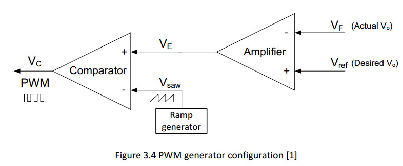
As shown in figure 3.4, PWM controller contains two main parts;
voltage error-amplifier and voltage comparator.
The error-amplifier compares the feedback voltage VF (applied to inverting input)
to reference voltage VREF (applied to non-inverting input)
then their difference which is called voltage error signal VE
after amplification is applied to noninverting input of voltage comparator.
Comparator compares this error voltage to sawtooth ramp VSAM that is generated by ramp generator,
if voltage VE is higher than VSAW output voltage of comparator goes high but
when VE is lower than VSAW the output of comparator goes low
to adjust the switching duty cycle.
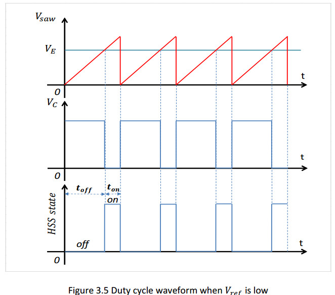
error voltage VE is inversely proportional to voltage reference VREF,
for example when VREF is low, error voltage VE is increased by error amplifier to adjust the switching duty cycle.
As can be seen in figure 3.5 when the error voltage is high the pulse width of PWM wave
at the output of voltage comparator (VC ) is increased to keep off High side switch (PMOS) for
the most time of the each cycle in order to reduce duty cycle to regulate output voltage.
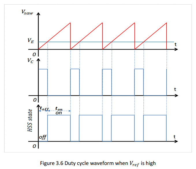
Vice versa as shown in figure 3.6 when VREF is high error amplifier reduces VE to keep on
the HSS for a most time of each period in order to adjust output voltage [14].
http://www.chinabaike.com/2011/0120/201049.html

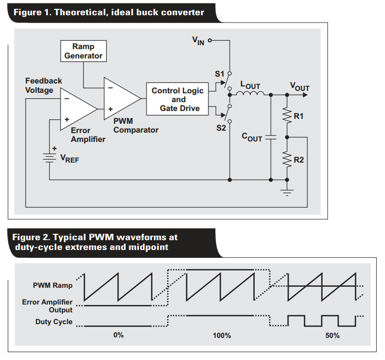
From the derivations for the boost, buck, and inverter (flyback), it can be seen that changing the duty cycle controls the steady-state output with respect to the input voltage. This is a key concept governing all inductor-based switching circuits.
The most common control method, shown in Figure 7, is pulse-width modulation (PWM). This method takes a sample of the output voltage and subtracts this from a reference voltage to establish a small error signal (VERROR). This error signal is compared to an oscillator ramp signal. The comparator outputs a digital output (PWM) that operates the power switch. When the circuit output voltage changes, VERROR also changes and thus causes the comparator threshold to change. Consequently, the output pulse width (PWM) also changes. This duty cycle change then moves the output voltage to reduce to error signal to zero, thus completing the control loop.
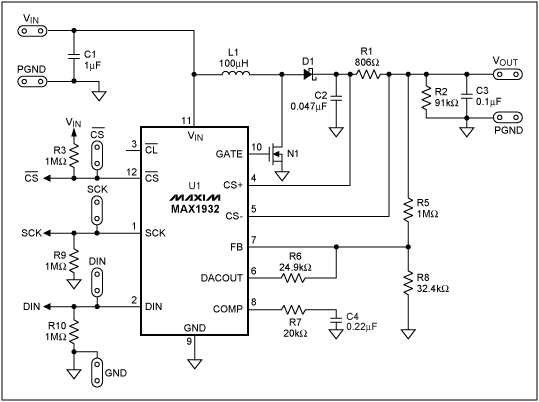
Figure 8 shows a practical circuit using the boost topology formed with the MAX1932.
This IC is an integrated controller with an onboard programmable digital-to-analog converter (DAC).
The DAC sets the output voltage digitally through a serial link.
R5 and R8 form a divider that meters the output voltage.
R6 is effectively out of circuit when the DAC voltage is the same as the reference voltage (1.25V).
This is because there is zero volts across R6 and so zero current.
When the DAC output is zero (ground), R6 is effectively in parallel with R8.
These two conditions correspond to the minimum and maximum output adjustment range of 40V and 90V, respectively.

Next, the divider signal is subtracted from the internal 1.25V reference and then amplified.
This error signal is then output on pin 8 as a current source.
This, in conjunction with the differential input pair, forms a transconductance amplifier.
This arrangement is used because the output at the error amp is high impedance (current source),
allowing the circuit's gain to be adjusted by changing R7 and C4.
This arrangement also provides the ability to trim the loop gain for acceptable stability margins.
The error signal on pin 8 is then forwarded to the comparator and output to drive the power switch.
R1 is a current-sense resistor that meters the output current.
When the current is unacceptably high, the PWM circuit shuts down, thereby protecting the circuit.
The type of switching (topology) in Figures 7 and 8 is classified as a voltage-mode controller (VMC)
because the feedback regulates the output voltage.
For analysis we can assume that if the loop gain is infinite, the output impedance for an ideal voltage source is zero.
Another commonly used type of control is current-mode control (CMC).
This method regulates the output current and, with infinite loop gain, the output is a high-impedance source.
In CMC, the current loop is nested with a slower voltage loop, as shown in Figure 9;
a ramp is generated by the slope of the inductor current and compared with the error signal.
So, when the output voltage sags, the CMC supplies more current to the load.
The advantage of CMC is its ability to manage the inductor current.
In VMC the inductor current is not metered. This becomes a problem because the inductor,
in conjunction with the output filter capacitor, forms a resonant tank that can ring and even cause oscillations.
Current mode control senses the inductor current to correct for inconsistencies.
Although difficult to accomplish, carefully selected compensation components can effectively cancel out this resonance in VCM.

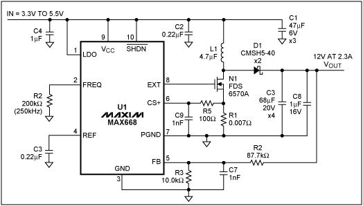
The circuit in Figure 10 uses CMC with the MAX668 controller.
This boost circuit is similar to Figures 7 and 8 except that R1 senses the inductor current for CMC.
R1 and some internal comparators provide a current limit.
R5 in conjunction with C9 filters the switching noise on the sense resistor to prevent false triggering of the current limit.
The MAX668's internal current-limit threshold is fixed; changing the resistor, R1, adjusts the current-limit setting.
The resistor, R2, sets the operating frequency.
The MAX668 is a versatile integrated circuit that can provide a wide range of DC-DC conversions.
The external components of the MAX668 can have high-voltage ratings that provide greater flexibility for high-power applications.
For portable applications that require less power, the MAX1760 and MAX8627 are recommended.
These latter devices use internal FETs, and sense the current by using the FETs' resistance to measure inductor current (no sense resistor required).
DC-DC converter Control techniques的更多相关文章
- PID DC/DC Converter Controller Using a PICmicro Microcontroller
http://www.microchip.com/stellent/idcplg?IdcService=SS_GET_PAGE&nodeId=1824&appnote=en011794 ...
- Practice safe dc/dc converter
Short-circuit protection is an obvious requirement for a power supply, especially when its load conn ...
- LT1946A-- Transformerless dc/dc converter produces bipolar outputs
Dual-polarity supply provides ±12V from one IC VC (Pin 1): Error Amplifier Output Pin. Tie external ...
- Simple dc/dc converter increases available power in dual-voltage system
The schematic in Figure 1 shows a way to increase the power available from a current-limited 5V supp ...
- Add margining capability to a dc/dc converter
You can easily add margining capability—that is, the ability to digitally adjust the output voltage— ...
- [专业名词·硬件] 2、DC\DC、LDO电源稳压基本常识(包含基本原理、高效率模块设计、常见问题、基于nRF51822电源管理模块分析等)·长文
综述先看这里 第一节的1.1简单介绍了DC/DC是什么: 第二节是关于DC/DC的常见的疑问答疑,非常实用: 第三节是针对nRF51822这款芯片电源管理部分的DC/DC.LDO.1.8的详细分析,对 ...
- DC/DC与LDO的差别
转自:http://bbs.eetop.cn/thread-459121-1-1.html 在平时的学习中,我们都有接触LDO和DC/DC这一类的电源产品,但作为学生的我们队这些东西可能了解不够深刻, ...
- DC DC降壓變換器ic 工作原理
目前DC/DC轉化器大致可分為:升壓型dc dc變化器.降壓型dc dc變化器及可升壓又可降壓dc dc變換器.我們今天主要提一下降壓型dc dc變換器的原理: 見下圖降壓變換器原理圖如圖1所示, 當 ...
- DC DC電路電感的選擇
注:只有充分理解電感在DC/DC電路中發揮的作用,才能更優的設計DC/DC電路.本文還包括對同步DC/DC及異步DC/DC概念的解釋. DCDC電路電感的選擇 簡介 在開關電源的設計中電感的設計為 ...
随机推荐
- SipDroid +miniSIPServer搭建SIP局域网语音通话(一)
最近在做语音通讯功能,参考下优秀开源软件SIPDroid好就这个了,svn check下最新的源代码 http://sipdroid.googlecode.com/svn/trunk/sipdroid ...
- Geoserver WFS跨域设置
测试版本为geoserver2.11.0. 两种方法都可以实现跨域设置: 第一种: 下载跨域jar包jetty-servlets.jar(下载geoserver使用的对应jetty版本——可以查看&l ...
- 百度2017春招<度度熊回家问题>
题目: 一个数轴上共有N个点,第一个点的坐标是度度熊现在位置,第N-1个点是度度熊的家.现在他需要依次的从0号坐标走到N-1号坐标.但是除了0号坐标和N-1号坐标,他可以在其余的N-2个坐标中选出一个 ...
- IndexWriterConfig的各个配置项说明(转)
1.Analyzer:分析器 2.matchVersion:所用Lucene的版本 3.ramBufferSizeMB:随机内存 默认为16M. 用于控制buffer索引文档的内存上限,如果buffe ...
- AtCoder Non-decreasing(数学思维)
题目链接:https://abc081.contest.atcoder.jp/tasks/arc086_b 题目大意:有n个数,最多可以执行2*n次操作,每次可以选择将ai加到aj上,最终使得该序列满 ...
- GDB调试实用命令
个人感觉从windows平台转到linux平台一个不适应的地方就是调试器的使用.因为windows下调试器基本上都依赖快捷键和图像界面来完成操作,就算是windbg这种伪命令行的工具,命令也很简单比较 ...
- SaltStack的salt-ssh使用及LAMP状态设计部署(五)
一.salt-ssh的使用 官方文档:https://docs.saltstack.com/en/2016.11/topics/ssh/index.html (1)安装salt-ssh [root@l ...
- LeetCode 118. 杨辉三角
118. 杨辉三角 给定一个非负整数numRows,生成杨辉三角的前numRows行. 在杨辉三角中,每个数是它左上方和右上方的数的和. 示例 输入: 5 输出: [ [1], [1,1], [1,2 ...
- Python并发编程-管道
管道的作用- 两个进程间传递消息 from multiprocessing import Pipe, Process def func(conn1,conn2): conn2.close() #子进程 ...
- Docker应用系列(四)| 部署java应用
本示例基于Centos 7,假设目前使用的账号为release,拥有sudo权限. 由于Docker官方镜像下载较慢,可以开启阿里云的Docker镜像下载加速器,可参考此文进行配置. 主机上服务安装步 ...