HBM内存介绍
原帖地址:http://www.anandtech.com/show/9969/jedec-publishes-hbm2-specification
The high-bandwidth memory (HBM) technology solves two key problems related to modern DRAM: it substantially increases bandwidth available to computing devices (e.g., GPUs) and reduces power consumption. The first-generation HBM has a number of limitations when it comes to capacity and clock-rates. However, the second-gen HBM promises to eliminate them.
JEDEC, a major semiconductor engineering trade organization that sets standards for DRAM, recently published the final specifications of the second-generation HBM (HBM2), which means that members of the organization had ratified the standard. The new memory technology builds upon the foundation of the original JESD235 standard, which describes stacked memory devices interconnected using through silicon vias (TSVs) with a very wide input/output (I/O) interface operating at moderate data-rates. The JESD235A will help engineers to further increase performance, capacity and capabilities of HBM memory chips. HBM Gen 2 will be particularly useful for the upcoming video cards by AMD and NVIDIA, which thanks to HBM2 can feature as much as 512 GB/s – 1 TB/s of memory bandwidth and 8, 16 or even 32 GB of memory onboard.
HBM Gen 1: Good, But With Limitations
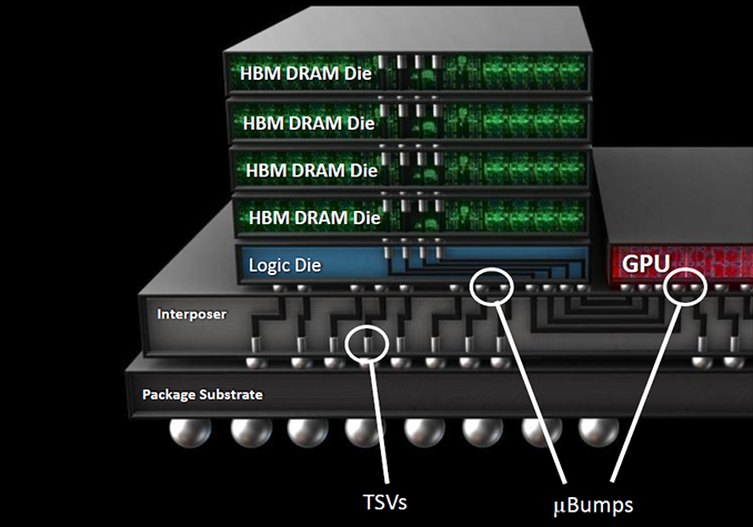
The original JESD235 standard defines the first-generation HBM (HBM1) memory chips with a 1024-bit interface and up to 1 Gb/s data-rate, which stack two, four or eight DRAM devices with two 128-bit channels per device on a base logic die. Each HBM stack (which is also called KGSD — known good stacked die) supports up to eight 128-bit channels because its physical interface is limited to 1024 bits. Every channel is essentially a 128-bit DDR interface with 2n prefetch architecture (256 bits per memory read and write access) that has its own DRAM banks (8 or 16 banks, depending on density), command and data interface, clock-rate, timings, etc. Each channel can work independently from other channels in the stack or even within one DRAM die. HBM stacks use passive silicon interposers to connect to host processors (e.g., GPUs). For more information about HBM check out our article called “AMD Dives Deep On High Bandwidth Memory — What Will HBM Bring AMD?”.
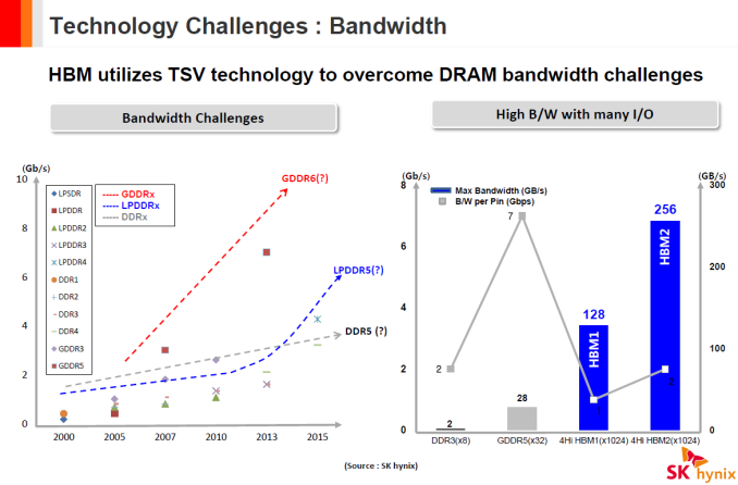
HBM gen 1 memory KGSDs produced by SK Hynix (the only company that makes them commercially) stack four 2 Gb memory dies and operate at 1 Gb/s data rate per pin. AMD uses these KGSDs with 1 GB capacity and 128 GB/s peak bandwidth per stack to build its Fiji GPU system-in-packages (SiPs) and the Radeon R9 Fury/R9 Nano video cards. The graphics adapters have 4 GB of VRAM onboard, not a lot for 2016. While AMD’s flagship video cards do not seem to have capacity issues right now, 4 GB of memory per graphics adapter is a limitation. AMD’s latest graphics cards sport 512 GB/s of memory bandwidth, a massive amount by today’s standards, but even that amount could be a constraint for future high-end GPUs.
HBM Gen 2: Good Thing Gets Better
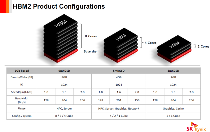
The second-generation HBM (HBM2) technology, which is outlined by the JESD235A standard, inherits physical 128-bit DDR interface with 2n prefetch architecture, internal organization, 1024-bit input/output, 1.2 V I/O and core voltages as well as all the crucial parts of the original tech. Just like the predecessor, HBM2 supports two, four or eight DRAM devices on a base logic die (2Hi, 4Hi, 8Hi stacks) per KGSD. HBM Gen 2 expands capacity of DRAM devices within a stack to 8 Gb and increases supported data-rates up to 1.6 Gb/s or even to 2 Gb/s per pin. In addition, the new technology brings an important improvement to maximize actual bandwidth.
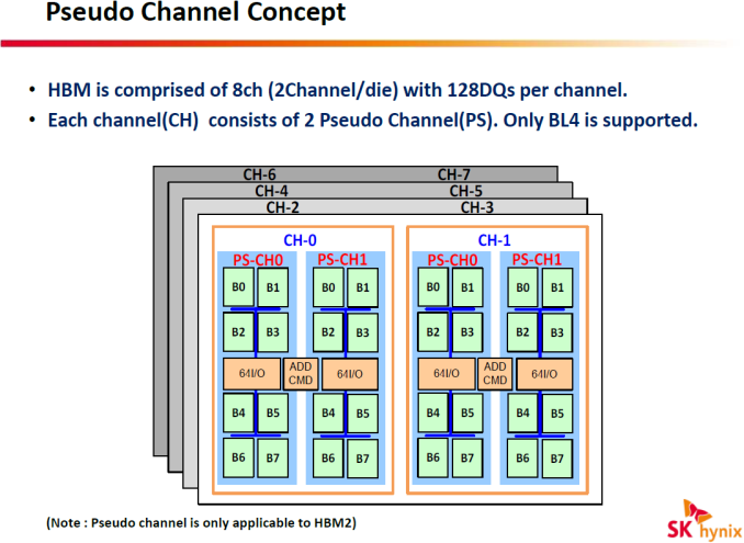
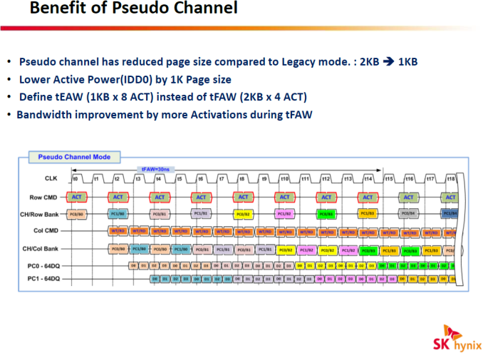
One of the key enhancements of HBM2 is its Pseudo Channel mode, which divides a channel into two individual sub-channels of 64 bit I/O each, providing 128-bit prefetch per memory read and write access for each one. Pseudo channels operate at the same clock-rate, they share row and column command bus as well as CK and CKE inputs. However, they have separated banks, they decode and execute commands individually. SK Hynix says that the Pseudo Channel mode optimizes memory accesses and lowers latency, which results in higher effective bandwidth.
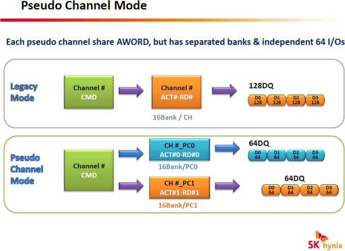
If, for some reason, an ASIC developer believes that Pseudo Channel mode is not optimal for their product, then HBM2 chips can also work in Legacy mode. While memory makers expect HBM2 to deliver higher effective bandwidth than predecessors, it depends on developers of memory controllers how efficient next-generation memory sub-systems will be. In any case, we will need to test actual hardware before we can confirm that HBM2 is better than HBM1 at the same clock-rate.
Additional improvements of HBM2 over the first-gen HBM includes lane remapping modes for hard and soft repair of lanes (HBM1 supports various DRAM cell test and repair techniques to improve yields of stacks, but not lane remapping), anti-overheating protection (KGSD can alert memory controllers of unsafe temperatures) and some other.
The second-generation HBM memory will be produced using newer manufacturing technologies than the first-gen HBM. For example, SK Hynix uses its 29nm process to make DRAM dies for its HBM1 stacks. For HBM2 memory, the company intends to use their 21nm process. Thanks to newer manufacturing technologies and higher effective bandwidth, HBM2 should have higher energy efficiency than HBM1 at its data-rates, but we do not have exact details at this point. In any case, HBM2 is likely to be more energy efficient than GDDR5 and GDDR5X, hence the odds are good that it will be the memory of choice for high-end graphics cards in the future.
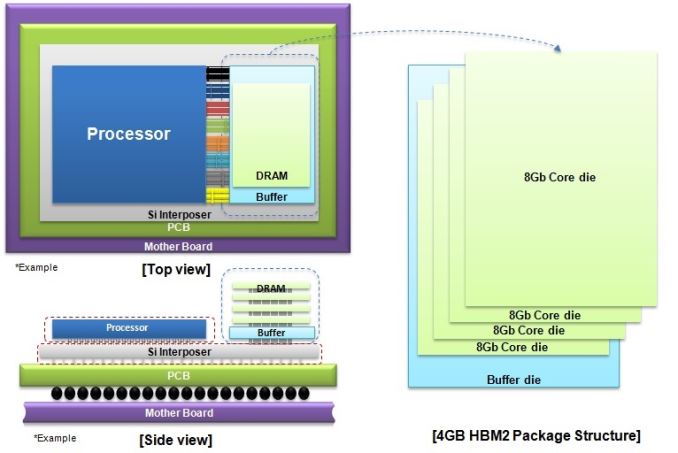
Samsung Electronics this week said that it had begun mass production of HBM2 memory, but did not reveal too many details. Samsung's HBM2 KGSD features 4 GB capacity, 2 Gb/s data rate per pin and is based on four 8 Gb DRAM dies. The memory chips will let device manufacturers build SiPs with up to 16 GB of memory. It is noteworthy that Samsung decided to use 8 Gb DRAM dies for its HBM2 stacks. Such decision looks quite logical since with 8 Gb DRAM ICs the company can relatively easily increase or decrease capacity of its KGSDs by altering the number of DRAM layers. The DRAM maker uses its 20nm process to produce its HBM2 DRAM KGSDs. Unfortunately, Samsung did not reveal actual power consumption of the new memory stacks.

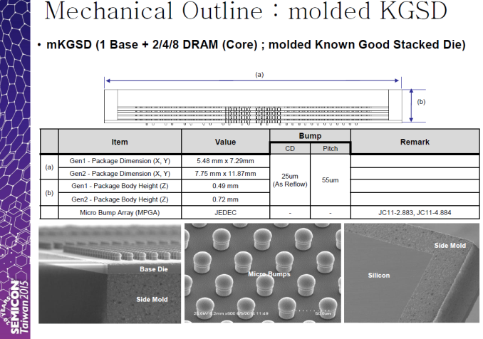
HBM2 memory stacks are not only faster and more capacious than HBM1 KGSDs, but they are also larger. SK Hynix’s HBM1 package has dimensions of 5.48 mm × 7.29 mm (39.94 mm2). The company’s HBM2 chip will have dimensions of 7.75 mm × 11.87 mm (91.99 mm2). Besides, HBM2 stacks will also be higher (0.695 mm/0.72 mm/0.745 mm vs. 0.49 mm) than HBM1 KGSDs, which may require developers of ASICs (e.g., GPUs) to install a heat-spreader on their SiPs to compensate for any differences in height between the memory stacks and GPU die, to protect the DRAM, and to guarantee sufficient cooling for high bandwidth memory.
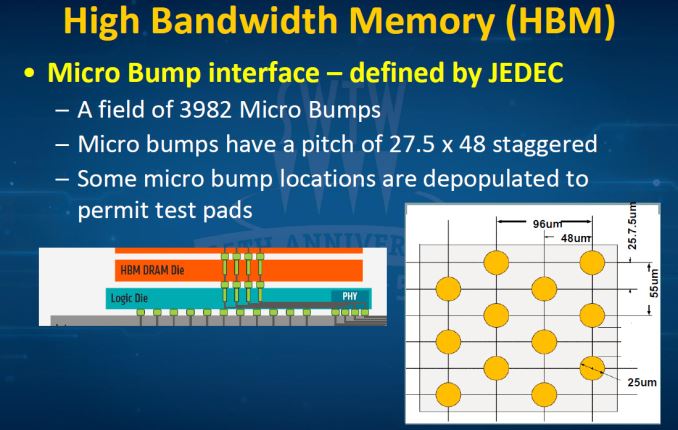
Larger footprint of the second-gen HBM2 means that the upcoming SiPs with multiple memory stacks will require larger silicon interposers, which means that they are going to be slightly more expensive than SiPs based on the first-gen HBM. Since geometric parameters of staggered microbump pattern of HBM1 and HBM2 are the same, complexity of passive silicon interposers will remain the same for both types of memory. A good news is that to enable 512 GB/s of bandwidth, only two HBM2 stacks are needed, which implies that from bandwidth per mm2 point of view the new memory tech continues to be very efficient.
A slide by FormFactor and Teradyne from their presentation at Semiconductor Wafer Test Workshop 2015
Since SK Hynix’s HBM1 KGSDs are smaller than the company’s HBM2 stacks, they are going to have an advantage over the second-gen high-bandwidth memory for small form-factor SiPs. As a result, the South Korea-based DRAM maker may retain production of its HBM1 chips for some time.
New Use Cases and Industry Support
Thanks to higher capacity and data-rates, HBM2 memory stacks will be pretty flexible when it comes to configurations. For example, it will be possible to build a 2 GB KGSD with 256 GB/s of bandwidth that will use only two 8 Gb memory dies. Such memory stack could be used for graphics adapters designed for notebooks or ultra-small personal computers. Besides, it could be used as an external cache for a hybrid microprocessor with built-in graphics (in the same manner as Intel uses its eDRAM cache to boost performance of its integrated graphics processors). What remains to be seen is the cost of HBM2 stacks that deliver 256 GB/s bandwidth. If HBM2 and the necessary interposer remains as expensive as HBM1, it will likely continue to only be used for premium solutions.
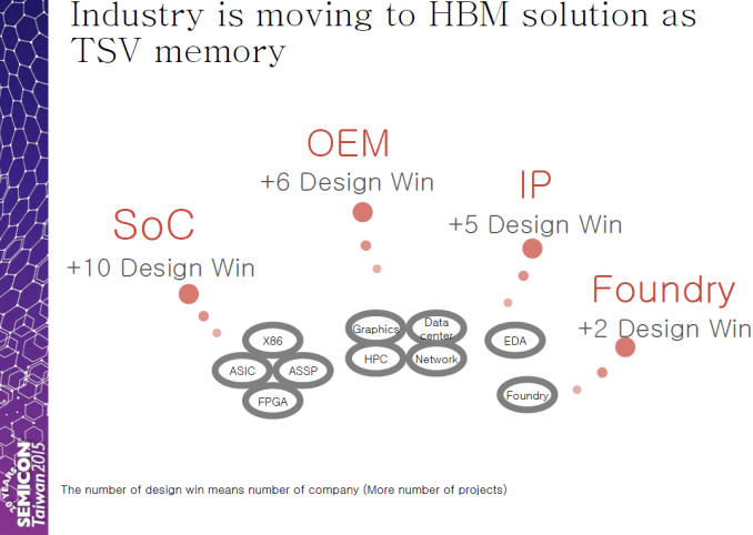
Thanks to a variety of KGSD configurations prepared by DRAM manufacturers, expect new types of devices to start using HBM2. Samsung and SK Hynix believe that in addition to graphics and HPC (high-performance computing) cards, various server, networking and other applications will utilize the new type of memory. As of September, 2015, more than 10 companies were developing system-on-chips (including ASICs, x86 processors, ASSPs and FPGAs) with HBM support, according to SK Hynix.
The first-generation HBM memory delivers great bandwidth and energy efficiency, but it is produced by only one maker of DRAM and is not widely supported by developers of various ASICs. By contrast, Samsung Electronics and SK Hynix, two companies that control well over 50% of the global DRAM output, will make HBM2. Micron Technology yet has to confirm its plans to build HBM2, but since this is an industry-standard type of memory, the door is open if the company wishes to produce it.
Overall, the industry support for the high bandwidth memory technology is growing. There are 10 companies working on SoCs with HBM support, leading DRAM makers are gearing up to produce HBM2. The potential of the second-gen HBM seems to be rather high, but the costs remain a major concern. Regardless, it will be extremely interesting to see next-generation graphics cards from AMD and NVIDIA featuring HBM2 DRAM and find out what they are capable of because of the new Polaris and Pascal architectures as well as the new type of memory.
HBM内存介绍的更多相关文章
- DRAM 内存介绍(三)
参考资料:http://www.anandtech.com/show/3851/everything-you-always-wanted-to-know-about-sdram-memory-but- ...
- DRAM 内存介绍(一)
转载自博客大神迈克老狼的blog: http://www.cnblogs.com/mikewolf2002/archive/2012/11/13/2768804.html 参考资料:http://ww ...
- Android mmap 文件映射到内存介绍
本文链接: Android mmap 文件映射到内存介绍 Android开发中,我们可能需要记录一些文件.例如记录log文件.如果使用流来写文件,频繁操作文件io可能会引起性能问题. 为了降低写文件的 ...
- DRAM 内存介绍(二)
参考资料:http://www.anandtech.com/show/3851/everything-you-always-wanted-to-know-about-sdram-memory-but- ...
- Java虚拟机的内存组成以及堆内存介绍
一.java内存组成介绍:堆(Heap)和非堆(Non-heap)内存 按照官方的说法:“Java 虚拟机具有一个堆,堆是运行时数据区域,所有类实例和数组的内存均从此处分配.堆是在 Java 虚拟机启 ...
- [ 转载 ] Java Jvm内存介绍
一.基础理论知识 1.java虚拟机的生命周期: Java虚拟机的生命周期 一个运行中的Java虚拟机有着一个清晰的任务:执行Java程序.程序开始执行时他才运行,程序结束时他就停止.你在同一台机器上 ...
- 干货长文:Linux 文件系统与持久性内存介绍
关注「开源Linux」,选择"设为星标" 回复「学习」,有我为您特别筛选的学习资料~ 1.Linux 虚拟文件系统介绍 在 Linux 系统中一切皆文件,除了通常所说的狭义的文件以 ...
- linux 内存介绍
linux用free -m 查看linux内存使用情况 具体参数如下: Mem:内存的使用情况总览表. totel:机器总的物理内存 单位为:M used:用掉的内存. free:空闲的物理内存. 物 ...
- System V共享内存介绍
(一)简单概念 共享内存作为一种进程间通信的方式,其相较于其他进程间通信方式而言最大的优点就是数据传输速率快.其内部实现的方式采用了Linux进程地址空间中的mmap文件映射区,将文件内容直接映射到各 ...
随机推荐
- [原]Jenkins(一)---我理解的jenkins是这样的
/** * lihaibo * 文章内容都是根据自己工作情况实践得出. *版权声明:本博客欢迎转发,但请保留原作者信息! http://www.cnblogs.com/horizonli/p/5330 ...
- jsp-javabean练习1
package javaBean; public class JavaB2 { private String name="lhy"; private int xuehao=123; ...
- HDU 1166 敌兵布阵 (数状数组,或线段树)
题意:... 析:可以直接用数状数组进行模拟,也可以用线段树. 代码如下: #pragma comment(linker, "/STACK:1024000000,1024000000&quo ...
- java线程详解(一)
1,相关概念简介 (1)进程:是一个正在执行的程序.每一个进程执行都有一个执行的顺序,该顺序就是一个执行路径,或者叫一个控制单元.用于分配空间. (2)线程:就是进程中一个独立的控制单元,线程在控制着 ...
- 在Openfire中使用自己的数据表之修改系统属性
通过修改Openfire安装目录的conf/openfire目录下是openfire.xml文件可以使用我们自定义的认证集成以及用户数据集成.其实仔细观察之后,在修改完配置文件再次启动openfire ...
- Android性能优化方法(六)
ContentProvider优化改进 1.索引简单的说,索引就像书本的目录,目录可以快速找到所在页数,数据库中索引可以帮助快速找到数据,而不用全表扫描,合适的索引可以大大提高数据库查询的效率.(1) ...
- [f]区间随机数函数
$.r = function(i, g) { var j = Math.random(), h = arguments.length; return h == 2 ? (i + Math.floor( ...
- EJB到底是什么,真的那么神秘吗??
1. 我们不禁要问,什么是"服务集群"?什么是"企业级开发"? 既然说了EJB 是为了"服务集群"和"企业级开发",那么 ...
- SQLSERVER 数据库性能的的基本
SQLSERVER 数据库性能的基本 很久没有写文章了,在系统正式上线之前,DBA一般都要测试一下服务器的性能 比如你有很多的服务器,有些做web服务器,有些做缓存服务器,有些做文件服务器,有些做数据 ...
- QSS总结以及最近做的Qt项目
什么是QSS QSS称为Qt Style Sheets也就是Qt样式表,它是Qt提供的一种用来自定义控件外观的机制.QSS大量参考了CSS的内容,只不过QSS的功能比CSS要弱很多,体现在选择器要少, ...