STM32F4: Generating parallel signals with the FSMC
STM32F4: Generating parallel signals with the FSMC
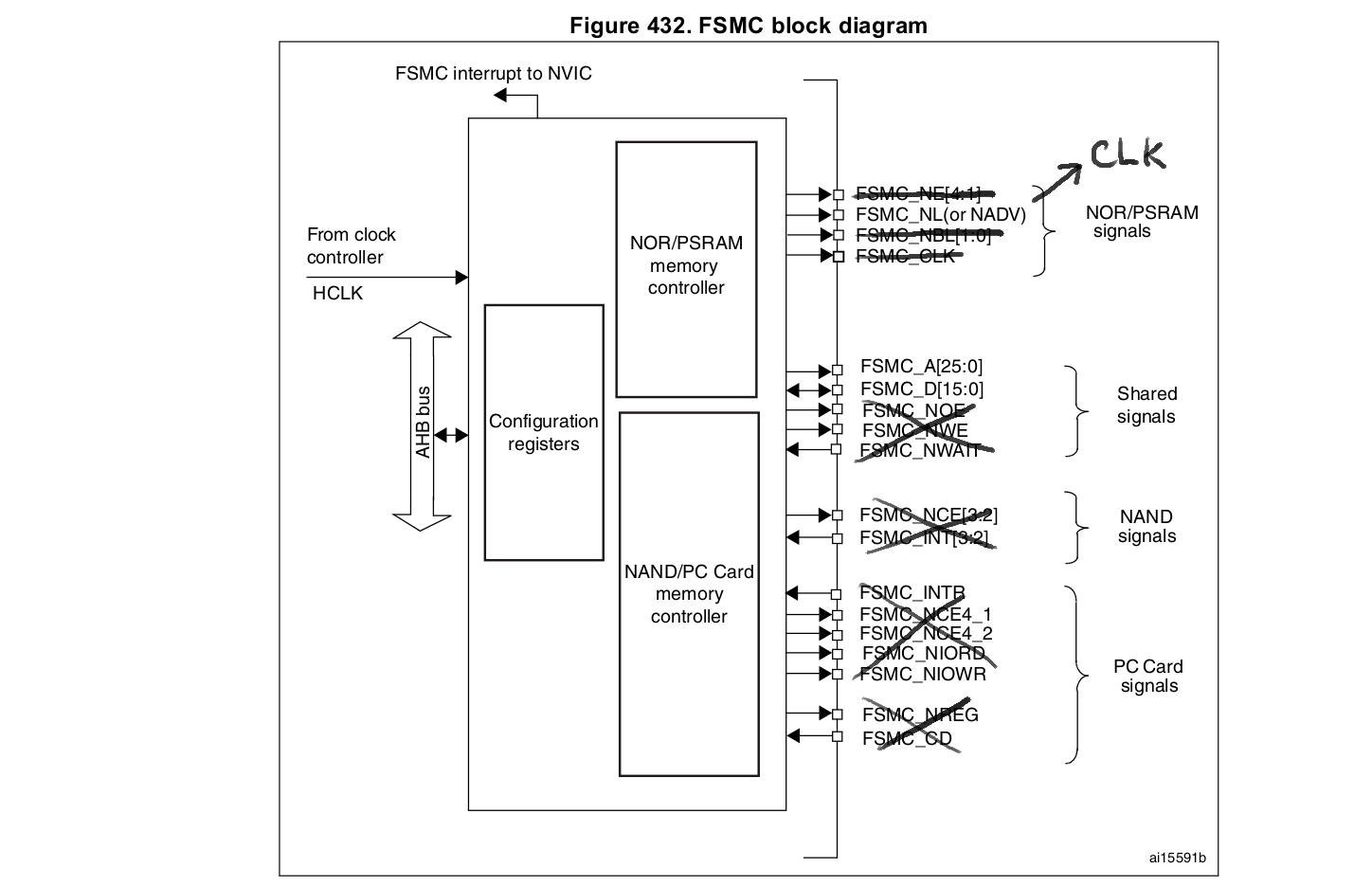
The goal: The memory controller can be used to generate a "generic" 16-bit parallel data stream with clock. Address generation will be disregarded, as well as other control signals dedicated to memory chips.
It must be noted that the STM32F40x and STM32F41x have the FSMC (static memories), while theSTM32F42x and STM32F43x have the FMC (static and dynamic memories). The differences between the two concern the support of SDRAM (dynamic RAM), address and data write FIFOs (both data and address, instead of data only for FSMC, and 16-word long instead of 2-word long only for FSMC), and the 32-bit wide data bus for FMC (See [1]).
Set pins (1st attempt)
Only data bus FSMC_D[15:0] and clock FSMC_CLK will be used (set as alternate function). The other pins are set as standard GPIOs (general purpose output).
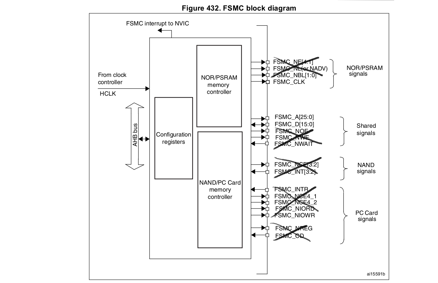
FSMC is alternate function 12 according to the datasheet (See "Table 9. Alternate function mapping" in [2]).
/* PD: 0, 1, 3, 8, 9, 10, 14, 15 -> alternate function (0b10) */

GPIOD->MODER = 0xA56A559A;

GPIOD->AFR[] = 0xCCCCCCCC; /* FSMC = AF12 (0xC) */

GPIOD->AFR[] = 0xCCCCCCCC;

/* PE: 7, 8, 9, 10, 11, 12, 13, 14, 15 -> alternate function (0b10) */

GPIOE->MODER = 0xAAAA9555;

GPIOE->AFR[] = 0xCCCCCCCC;

GPIOE->AFR[] = 0xCCCCCCCC;
FSMC setup/init (1st attempt)
Be careful of the the wicked register map documentation of the FSMC block:
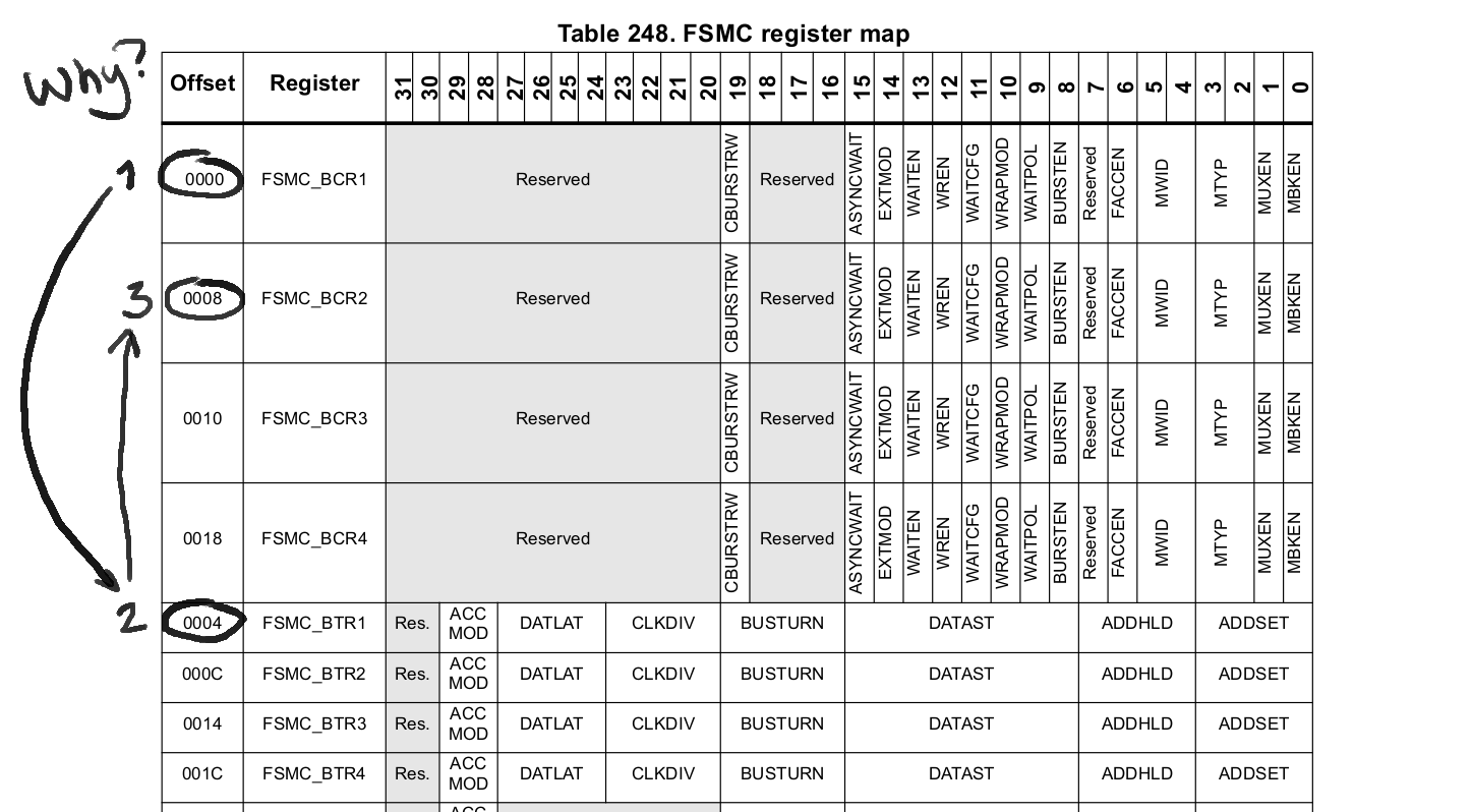
This is very misleading, since all other table are ordered as found in memory, but not here.
/* PSRAM, synchronous (burst), non-multiplexed */

/* control register */

FSMC_Bank1->BTCR[] = FSMC_BCR1_CBURSTRW | FSMC_BCR1_WAITPOL | FSMC_BCR1_BURSTEN | FSMC_BCR1_MWID_0 | FSMC_BCR1_WREN | FSMC_BCR1_MTYP_0 /* PSRAM */ | FSMC_BCR1_MBKEN;

/* timing register */

FSMC_Bank1->BTCR[] = FSMC_BTR1_CLKDIV_1 /* div 3 */ ;
It is noticable that the timing are all set to 0, except the clock.
Result (1st attempt)
The code writing to the FSMC is using an array and simulate a sequencial memory request, in order to take advantage of the burst mode.
volatile uint16_t* fsmc = (uint16_t*)0x60000000;

for(uint32_t i=; i<(sizeof(bitstream_bin)/); i++) {

        uint16_t w = ((uint16_t*)bitstream_bin)[i];

        fsmc[i] = w;

}
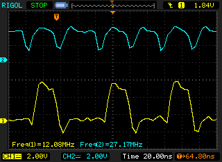
The clock is ~54MHz, but the maximum clock is HCLK/2 = 168/2=84MHz. Unfortunately, my oscilloscope is too slow for this.
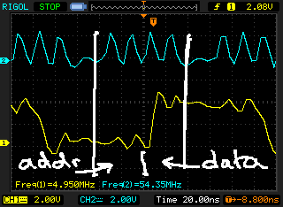
At least, 4 clock cycles are required to write one data. Data latency (DATLAT lowest value is 2). There is one cyle to give the address, two cyle of latency, one cyle for give the data.
At max FSMC speed (~84MHz), after dividing the clock by 4, the 16-bit parallel transmission would only be ~20MHz.

Bursts are possible up to 32 bits (two 16-bit data words). When using this feature, two data words are send for each address, hence more data is sent, but the clock is hard to use: 3 ticks for the (empty) address, 1 tick for the first data, 1 tick for the second data (5 cycles for 2 data, ~30MHz max).
Set pins (2nd attempt)
/* PD: 0, 1, 8, 9, 10, 14, 15 -> alternate function (0b10) */

GPIOD->MODER = 0xA56A555A;

GPIOD->AFR[] = 0xCCCCCCCC; /* FSMC = AF12 (0xC) */

GPIOD->AFR[] = 0xCCCCCCCC;

/* PE: 7, 8, 9, 10, 11, 12, 13, 14, 15 -> alternate function (0b10) */

GPIOE->MODER = 0xAAAA9555;

GPIOE->AFR[] = 0xCCCCCCCC;

GPIOE->AFR[] = 0xCCCCCCCC;

/* PB: 7 -> AF */

GPIOB->MODER = 0x55551555;

GPIOB->AFR[] = 0xCCCCCCCC;

GPIOB->AFR[] = 0xCCCCCCCC;
FSMC setup/init (2nd attempt)
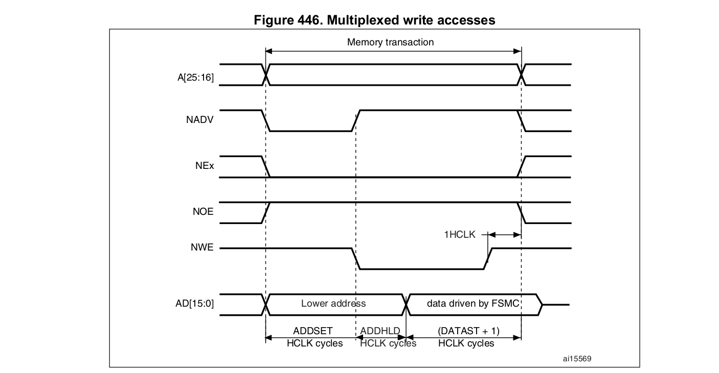
/* NOR flash, asynchronous, multiplexed */

/* control register */

FSMC_Bank1->BTCR[] = FSMC_BCR1_WREN | FSMC_BCR1_FACCEN | FSMC_BCR1_MWID_0 /* 16-bit */ | FSMC_BCR1_MTYP_1 /* NOR flash */ | FSMC_BCR1_MUXEN | FSMC_BCR1_MBKEN;

/* timing register */

FSMC_Bank1->BTCR[] = FSMC_BTR1_CLKDIV_0 | FSMC_BTR1_DATAST_0 | FSMC_BTR1_ADDHLD_0 | FSMC_BTR1_ADDSET_1;
Result (2nd attempt)
We want to use the NADV signal as a new clock CLK.
volatile uint16_t* fsmc = (uint16_t*)0x60000000;

uint16_t w[] = {

        0xFFFF, 0x0000, 0xFFFF, 0x0000,

        0xFFFF, 0x0000, 0xFFFF, 0x0000};

for(uint32_t i=;i<;i++) {

        fsmc[] = w[i];

}
We write to the same address in order to force a new memory transaction and cycle NADV.
The problem is that the data bus is updated after the positive edge of the NADV "clock". This issue can be overcome by multiplexing the address and data bus and put the data value as address. The ADDSET value is also increased in order to have a more balanced clock (ADDSET=3).
for(uint32_t i=;i<;i++) {

        uint16_t v = w[i];

        fsmc[v] = v;

}
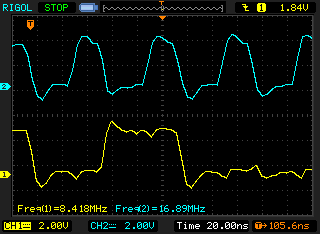
Unfortately, the overall clock speed decreased because the address "trick".
Conclusion
A "nice looking" 16-bit parallel signal with clock can be generated at approx. 16MHz using the memory controller (FSMC) in asynchronous NOR Flash mode. 20MHz can be achieved with an external clock divider (div 4) in synchronous PSRAM mode. If the clock edge can be aligned with the data edge, 27MHz is possible from SRAM.
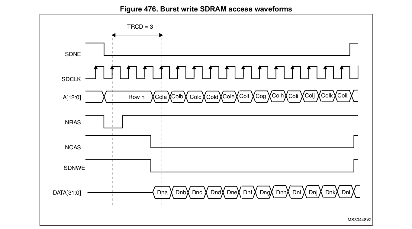
Note: the FMC (Flexible Memory Controller, also supporting SDRAM) in SDRAM mode can generate a synchronous burst of one data per clock. In this case, 84MHz is possible in theory. I haven't the hardware to test it.
STM32F4: Generating parallel signals with the FSMC的更多相关文章
- STM32F4: GENERATING A SINE WAVE
http://amarkham.com/?p=49
- Flexible implementation of a system management mode (SMM) in a processor
A system management mode (SMM) of operating a processor includes only a basic set of hardwired hooks ...
- PMP用语集
AC actual cost 实际成本 ACWP actual cost of work performed 已完工作实际成本 BAC budget at completion 完工预算 BCWP b ...
- 论文翻译:2021_DeepFilterNet: A Low Complexity Speech Enhancement Framework for Full-Band Audio based on Deep Filtering
论文地址:DeepFilterNet:基于深度滤波的全频带音频低复杂度语音增强框架 论文代码:https://github.com/ Rikorose/DeepFilterNet 引用:Schröte ...
- STM32F4—fsmc的配置步骤
0:开启GPIO时钟和FSMC时钟 1:配置GPIO 2:配置片选控制寄存器 3:配置片选时序寄存器 4:配置写入时序寄存器 GPIO_InitTypeDef GPIO_InitStructure;/ ...
- STM32F4 SPI with DMA
STM32F4 SPI with DMA A few people have requested code, so I thought I’d post the code showing how I’ ...
- Generating Complex Procedural Terrains Using GPU
前言:感慨于居然不用tesselation也可以产生这么复杂的地形,当然致命的那个关于不能有洞的缺陷还是没有办法,但是这个赶脚生成的已经足够好了,再加上其它模型估 计效果还是比较震撼的.总之好文共分享 ...
- GNU Parallel Tutorial
GNU Parallel Tutorial Prerequisites Input sources A single input source Multiple input sources Linki ...
- Massively parallel supercomputer
A novel massively parallel supercomputer of hundreds of teraOPS-scale includes node architectures ba ...
随机推荐
- Hash::make与Hash::check
调用方法之前要先去引用: use Illuminate\Support\Facades\Hash; 可以调用 Hash 门面上的 make 方法对存储密码进行哈希: $pwd = Hash::make ...
- python 多进程的启动和代码执行顺序
对照着廖雪峰的网站学习Python遇到些问题: 在进程中,父进程创建子进程时发现,显示不是按照顺序显示,疑问? 参照代码如下: from multiprocessing import Pool imp ...
- 【Udacity并行计算课程笔记】- lesson 1 The GPU Programming Model
一.传统的提高计算速度的方法 faster clocks (设置更快的时钟) more work over per clock cycle(每个时钟周期做更多的工作) more processors( ...
- python3之模板pycurl探测web服务质量
1.pycurl简介 pycURL是libcurl多协议文件传输库的python接口,与urllib模块类似,PycURL可用于从python程序中获取由URL标识的对象,功能很强大,libcurl速 ...
- shell函数中eof报错(warning: here-document at line 9 delimited by end-of-file (wanted `EOF'))
在shell编写函数时,函数中有eof和EOF,如果是在sublime编写按照格式tab缩进会有以下报错 解决办法: 取消函数中的tab缩进,在运行即可
- 014_mac下的端口查看
一. 使用netstat去过滤listen效果不怎么理想. $ netstat -an|grep -i --color "listen" tcp6 0 0 ::1.5601 *.* ...
- makefile 中 foreach
四.foreach 函数 foreach函数和别的函数非常的不一样.因为这个函数是用来做循环用的,Makefile中的foreach函数几乎是仿照于Unix标准Shell(/bin/sh)中的for语 ...
- selenium玩转svg操作
今天写脚本发现页面有svg结构,里面的元素无法定位,查找很多资料,然后就记录下来 初步尝试直接在页面中获取svg中包含元素的xpath,直接利用selenium方法访问,无法捕获到相关元素信息. SV ...
- .NetCore Cap 结合 RabbitMQ 实现消息订阅
开源分布式消息框架 Cap 可以在GitHub上拉也可以通过nuget添加 上一篇博文写了 Windows RabbitMQ的安装使用 Cap支持事务,通过捕获数据库上下文连接对象实现 消息事务,消息 ...
- 【LOJ】#2549. 「JSOI2018」战争
题解 仔细分析了一下,如果写个凸包+每次暴力半平面交可以得到70分,正解有点懵啊 然后用到了一个非常结论,但是大概出题人觉得江苏神仙一个个都可以手证的结论吧.. Minkowski sum 两个凸包分 ...