High Voltage Boost Supply
http://learn.adafruit.com/ice-tube-clock-kit/design
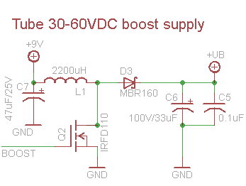
Tubes such as VFDs, Nixies, Decatrons, etc require high voltage to light the gas in the tube. For nixies, this iabout 170VDC. VFDs aren't as bad they only need about 30-50VDC. In order to reduce cost, we use the microconrtoller to make a boost converter and avoid paying $5 for a seperate chip. We can do this because we don't need a precision output and the current draw is mostly constant. The boost regulator is run open-loop there is no feedback resistor divider as it isn't necessary as long as the input voltage is within a reasonable range.
The boost circuit works by connecting the power inductor L1 to ground that current can flow through it by turning on Q2. After a little bit of time, we disconnect the from ground (by turning off Q2) this means that there is no longer a path for the current in L1 to flow to ground. When this happens, the voltage across the inductor increases (this is the electric property of inductors) and charges up C6 . When the voltage increases to the level we want it to be (30V+) we turn on Q2 again which allows the current in L1 to flow back to ground. If we do this fast enough, and C6 large enough, the voltage on C6 is smoothed out and we get a nice steady high voltage.
The timing of turning off/on Q2 allows us to modify the output voltage. Normally there is a feedback resistor to the microcontroller but it is not here because we are running it open-loop. To drive Q2 we use the PWM output from the microcontroller and adjust the duty cycle to vary brightness.
- The voltage in is nominally 9 to 12VDC
- The current draw for the IV-18 tubes is about 8mA per digit and 11mA for the grid. Remember, though, that we only light up one digit at a time! So we need about 20mA total (we also meaured this in-circuit to verify)
- The voltage output is going to be between 30V-50V (its really much too bright after that point)
- The PWM output speed of the microcontroller is F_CPU / 256 = 8 MHz / 256 = 31.25KHz (period of 32 useconds)
With this information we can calculate the inductor size and capacity!
The optimal transfer between Vin and Vout is:
Vo/Vi = 1 / (1-D) where D is the duty cycle.
Solving for D = 1 - (Vi/Vo) and plugging in numbers:
For Vo = 50V and Vi = 9V, D = 82% (maximum)
For Vo = 30V and Vi = 12V D = 60% (minimum)
So the duty range will be between 60% and 82%. That would correspond to between ~150 and 220 out of 256, but note that when the PWM signal islow the switch is on so we need to invert that to a range of about 36 to 106 (in the code we actually use about 20 to 90).
OK so our PWM range is good, we just want to keep it between around 10% and 90% which we do.
Next, we need to make sure that the inductor continuously dumps current into C6 the entire time Q2 is off (continuous conduction mode). This is dependant on a lot of variables:
D*T*Vin/(2*L) < iout/(1-D)
Note that T is period time and is = 1/frequency. Solving for L, we choose the lowest duty cycle which will give us the upper bound for the inductor:
D*Vin * (1-D) / (freq * 2 * Iout ) < L
D = 60% (0.6)
iout = 20mA (0.02 Amp)
Vin = 12V nominal
1/T = freq = 31250 HzL > 0.6 * 12 * (1 - 0.6) / (31250* 2 * 0.02)
L > 2304 uH
This is our upper limit, so lets just say L = 2200uH (a standard value). Note that for 9V->60 we need L > 918uH which is our lower bound and our average case is a duty cycle of about 70% which is 1500uH.
We also want to make sure that we have a enough current capacity, so lets calculate the maximum current that builds up in the inductor. We now have to pick this for the -smallest- inductor, in the case of 9V boosting to 50V, an 82% duty cycle.
Ipk = (Vin * D)/(f * L)
Ipk = (9 * 0.82)/(31250 * .001) = 0.24 Amp
So! We want to make sure our inductor is > 2200 uH and will not saturate below 0.24 A.
The important thing to note here is that, for a given package (size) of inductor, the higher the inductance the lower the current capability.
Since this is a through-hole kit, we have to stick with a radial/axial inductor.
Searching Mouser for power inductors, we find the RLB9012 family (datasheet) which is the same type used in the mintyboost. This is a good inductor family, lets check out the range.
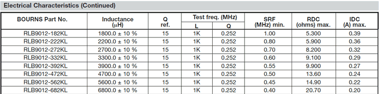
t looks like we're good to go with this group of inductors as the max current capacity of the 2200uH is well above our minimum 0.25 Any value higher than that will be OK as the Ipk will fall faster than the IDCmax
In reality, you don't need such high inductances because our system is not running on a battery and doesn't require a great power supply with low ripple and good efficiency. Inducances 270uH and lower worked just fine, the converter is operating in discontinuous mode which is not as efficient. Its also not as easy to calculate the precise specifications. Luckily this is a very indiscriminate tube and is cool with ripple and voltage fluctuations.
The diode is a schottky type, and needs to have a breakdown voltage larger than the maximum boost voltage (in this case 60V) we're usingMBR160 with 60V breakdown.
One way to improve the design to reduce the size and power requirements of the inductor is to increase the frequency. Doubling the frequency halves the required inductance and current requirements of the inductor!
I have a nice little calculator if you want to design your own basic boost converter
Thanks tons to Riad at jfet.org for the idea and calculations! (He has some great clock designs, so check them out)
For more information on boost converters see this article on wikipedia.
http://en.wikipedia.org/wiki/Boost_converter
A boost converter (step-up converter) is a DC-to-DC power converter with an output voltage greater than its input voltage. It is a class of switched-mode power supply (SMPS) containing at least two semiconductor switches (a diode and a transistor) and at least one energy storage element, a capacitor, inductor, or the two in combination. Filters made of capacitors (sometimes in combination with inductors) are normally added to the output of the converter to reduce output voltage ripple.
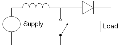
The basic schematic of a boost converter. The switch is typically a MOSFET, IGBT, or BJT.
http://learn.adafruit.com/diy-boost-calc
For many small projects, its cheaper and easier to DIY a boost converter than to buy a specialty chip. DIY converters are usually not as efficient but they're quick & cheap!
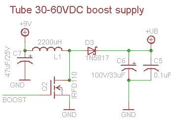
The above schematic section shows how I designed a 30-60V vacuum fluorescent tube display driven from a microcontroller pin.
Tubes such as VFDs, Nixies, Decatrons, etc require high voltage to light the gas in the tube. In order to reduce cost, we use a microconrtoller to make a boost converter and avoid paying $5 for a seperate chip. We can do this because we don't need a precision output and the current draw is mostly constant. The boost regulator is run open-loop there is no feedback resistor divider as it isn't necessary as long as the input voltage is within a reasonable range
The microcontroller runs at 8MHz so the 8-bit PWM output is 31250 Hz. The inductor and output capacitor is calculated below. The diode is a standard Schottkey type, but make sure you specify one that can handle the full voltage difference and peak current. The switch just has to be able to handle the max voltage plus some for safety. Note that this design is meant for 'static' output currents, not for variable current draw designs. There is no feedback and its very approximate! This is not for precision electronics!
The boost circuit works by connecting the power inductor L1 to ground that current can flow through it by turning on Q2. After a little bit of time, we disconnect the inductor from ground (by turning off Q2) this means that there is no longer a path for the current in L1 to flow to ground. When this happens, the voltage across the inductor increases (this is the electric property of inductors) and charges up C6 . When the voltage increases to the level we want it to be (30V+) we turn on Q2 again which allows the current in L1 to flow back to ground. If we do this fast enough, and C6 large enough, the voltage on C6 is smoothed out and we get a nice steady high voltage
The timing of turning off/on Q2 allows us to modify the output voltage. Normally there is a feedback resistor to the microcontroller but it is not here because we are running it open-loop. To drive Q2we use the PWM output from the microcontroller and adjust the duty cycle to vary brightness.
These sorts of designs can be easily made with a 555, once you have the PWM output, connect it up toQ2!
http://learn.adafruit.com/diy-boost-calc/the-calculator
http://learn.adafruit.com/downloads/pdf/diy-boost-calc.pdf
High Voltage Boost Supply的更多相关文章
- OpAmp Voltage Follower/Regulator
LDO Regulator High accuracy voltage regulator Vout = 2.5V * (1 + ( 5.6 / 6.8 ) ) = 4.55V Recently th ...
- OBD Experts OBD II Software OBD II Protocol Stack
http://www.obdexperts.co.uk/stack.html OBD II Software OBD Experts can provide you with ready to use ...
- 【转】linux设备驱动之MMC SD卡——核心层简单分析
原文网址:http://blog.chinaunix.net/uid-28685940-id-3889878.html /*************************************** ...
- An Isolated DAC Using PWM Output
An Isolated DAC Using PWM Output Arduino‘s (ATmega328P) PWM outputs via analogWrite can be convenien ...
- RF layout check list
Analog-digital circuit 1. Insure C36 and C33 placed next to each other to avoid open stubs 2. Keep U ...
- Use two picogate devices for bidirectional level-shifting
In new mixed-voltage systems, it is often necessary to level-shift a control signal from a high leve ...
- PatentTips - Integrated circuit well bias circuitry
1. Field of the Invention This invention relates in general to an integrated circuit and more specif ...
- Get just enough boost voltage - current-mirror circuit - VOUT tracks VIN varies
Adding a current-mirror circuit to a typical boost circuit allows you to select the amount of boost ...
- BOOST Converter Analog/Digital Adjusted Output Voltage TPS61045 MAX1932
DIGITALLY ADJUSTABLE BOOST CONVERTER The TPS61045 is a high frequency boost converter with digitally ...
随机推荐
- 如何学习React--[转]
如果你是一个 React (或者前端) 新手, 出于以下的原因, 你可能会对这个生态圈感到困惑: React 的目标群体历来是喜欢尝试新事物的开发者和前端专家. Facebook 只开源了他们在实际使 ...
- dede导航栏目调用
1.基础调用 {dede:channel row='5' type ='top' } <li><a href="[field:typelink/]">[fi ...
- 关于jedis2.4以上版本的连接池配置,及工具类
jedis.propertise 注意以前版本的maxAcitve和maxWait有所改变,JVM根据系统环境变量ServerType中的值 取不同的配置,实现多环境(测试环境.生产环境)集成. re ...
- 出现丢包解决方法(ping: sendmsg: Operation not permitted)
故障排查: 早上突然收到nagios服务器check_icmp的报警,报警显示一台网站服务器的内网网络有问题.因为那台服务器挂载了内网的NFS,因此内网的网络就采用nagios的check_icmp来 ...
- 全方位掌握nsis脚本
NSIS 确实是一个不错的安装程序制作软件.新版本 2.0a7 真正实现了中文支持和支持 WinXP 的安装对话框. 不过要用它实现漂亮的安装界面和完美的安装功能就必须好好的写脚本. 而 NSIS 的 ...
- Ansible条件测试
本节内容: Ansible条件测试 一.Ansible条件测试 在ansible中还可以进行条件测试.如果需要根据变量.facts或此前任务的执行结果来做为某task执行与否的前提时要用到条件测试. ...
- Rookey.Frame之系统初始化
昨天介绍了数据库的配置,今天继续介绍系统的初始化功能:针对系统初始化在开发中也是很重要的一部分,它可以提前将相关数据提前自动初始化到系统中,同时也可以为上线测试提供方便,可以很方便进行系统测试演练,防 ...
- SQLite数据库、ListView控件的使用
android下数据库的创建(重点) 在Android平台上,集成了一个轻量级嵌入式关系型数据库—SQLite,SQLite3支持 NULL.INTEGER.REAL(浮点数字).TEXT(字符串文本 ...
- Bootstrap--响应式显示图片信息列表
HTML布局 <link href="~/Content/StyleSheet1.css" rel="stylesheet" /> <div ...
- 华三IRF的配置
https://blog.csdn.net/VictoryKingLIU/article/details/79255901 拓扑结构 1 配置成员编号(重启) 2 配置成员优先级(大的主设备) 3 配 ...