ARM Cortex Design Considerations for Debug
JTAG was the traditional mechanism for debug connections for ARM7/9 parts, but with the Cortex-M family, ARM introduced the Serial Wire Debug (SWD) Interface. SWD is designed to reduce the pin count required for debug from the 5 used by JTAG (including GND) down to 3. In addition, one of the pins freed up by this can be used for the low cost SWO tracing technology - for more details see the FAQ "Overview of Trace support in LPCXpresso IDE".
The SWD/SWV pins are overlaid on top of the JTAG pins as follows:
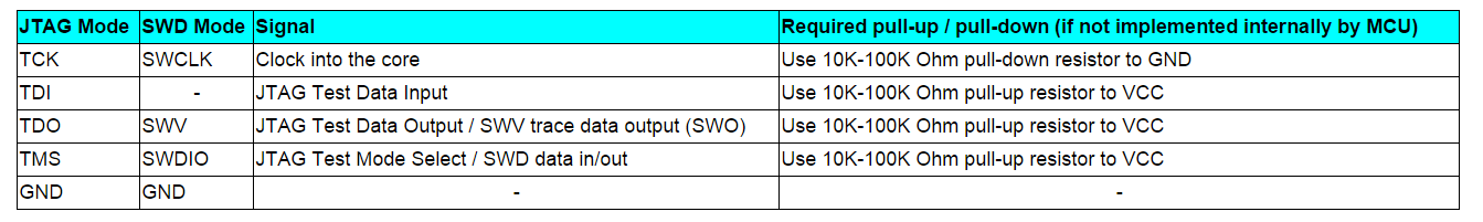
Some MCUs do not include internal pull-up or pull-down resistors on JTAG/SWD pins. You will need to review the datasheet for the specific MCU being used to confirm. Where internal resistors are not provided, these should be added externally onto your board as detailed above. You may use resistors between 10K and 100K for these signals. This will prevent the signals from floating when they are not connected to anything. Failure to do this will lead to, at best, unreliable debug connections, or more likely no ability to debug at all.
If an internal resistor is provided for a pin by the MCU, then an external resistor is not required for that pin. But if external resistor is provided in such cases, then it must match that provided internally by the MCU.
Note for TCK/SWCLK, although a pull-down is recommended, you can alternatively use a pull-up. The main thing is that it does not float. Note in particular that if the MCU provides an internal pull-up on this signal, then adding an external pull-down on the board is not recommended.
Note that Cortex-M0/M0+ parts does not support SWV trace.
Other important debug related signals
When designing your board, you should also take the following signals into account for debug purposes. Failure to do this will lead to, at best, unreliable debug connections, or more likely no ability to debug at all.
- RESET
- Connect this pin to the (active low) reset input of the target MCU
- We would strongly recommend also including RESET in addition to SWDIO, CLK and GND. For debugging, the tools may try to pull this in certain circumstances (depending upon debug probe, debug configuration settings and tools).
- ISP
- Most NXP MCU's have an ISP pin which (when pulled low) can be used to cause the MCU to enter a bootloader on reset.
- For example on LPC17xx this is P2.10 and on LPC11xx and LPC13xx it is P0.1.
- Always ensure that you have a 10K to 100K Ohm pull up resistor on the ISP pin, otherwise you are unlikely to be able to make a successful debug connection.
- VTref
- The Voltage Target Reference pin supplies some debug probes (such as LPC-Link2) with the debug rail voltage of the target to match its I/O logic level. For more information, see "Logic Levels and Ground" below.
- RTCK, DBGSEL
- Some NXP LPC2000 devices have special pins that enable the JTAG interface. For example, on the NXP LPC2129 the signal RTCK must be driven low during RESET to enable the JTAG interface. You may want to add jumpers to your hardware to accomplish this.
Logic Levels and Ground
VTref (the Voltage Target Reference pin, direction from target to debug probe) supplies some debug probes such as LPC-Link2 and Red Probe+ with the debug rail voltage of the target to match its I/O logic level. VTref can be tied directly to the target VDDIO rail or through a resistor. If VTref is tied high through a resistor, its value must be no greater than 100Ω.
The original LPC-Link1 only supported 3.3V and did not require VTref whereas the LPC-Link2 uses dual-supply buffers that allows the Link2 to work with targets using a different voltage (between 1.8V - 4.3V).
On the LPC-Link2, when JP2 is shunted this will power the target side of the dual-supply buffer and provide power to the target through a diode on VTref. With JP2 open the target must supply the VTref to power the target side of the dual-supply buffer.
When a debug probe attempts to adjust logic levels based on the voltage it sees on VTref, this is referenced to whatever GND it has to work with. The voltage at VTref is coming from your target, thus you need a good GND, shared with your target hardware.
Note that debug probes can be killed (like most USB devices) by excessive over current through ground of the probe and back through the PC used for debugging. The usual cause of this is that your target has it's own PSU and has a ground differential slightly different from your debug PC. Please do not rely on your debug probe to ground your PC to the same potential as your target.
Power
Even when you have designed your debug circuit according to the above considerations, you should also check that sufficient power is being supplied to your target in order to obtain a reliable debug connection. If you are using a USB port on your PC to power your target, make sure that your PC is able to supply the required power over USB - many PC USB ports do not meet USB power requirements.
Debug Connector Pinouts
ARM has defined three debug connector pinouts that are in common use, a "traditional" 20 pin connector, a Cortex 10 pin connector and a Cortex 20 pin Debug+ETM connector...
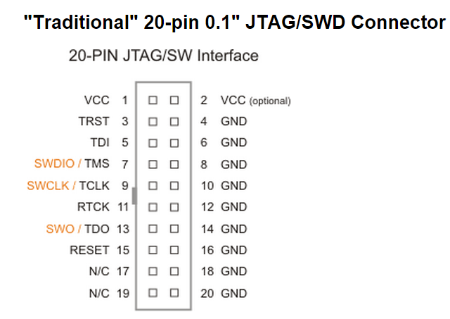
- This connector was originally defined for connection to ARM7/9 parts over JTAG, but is still sometimes found in Cortex-M systems (for connections over JTAG or SWD).
- Note that RTCK (Return clock) is only used on older ARM cores (ARM7TDMI and ARM9 family) before the debug was properly decoupled from the core clock domain.
- Dimensions of the ARM JTAG connector are 1.29" x 0.722" (33mm x 18.5mm).

- Suitable connector headers include :
- Harwin: M50-3500542
- Mouser: 855-M50-3500542
- Samtec shrouded header: FTSH-105-01-F-D-K
- The 10-pin Samtec FTSH-105-01 connector has the dimensions: 0.25" x 0.188" (6.35mm x 4.78mm).
- Some boards use un-shrouded 10-pin headers. Always ensure that you connect your cable correctly, typically by matching the "1" marked on the board to the red -stripe on the cable.
- The 10-pin cable is Samtec part number FFSD-05-D-12.00.01-N

- This small 20-pin (0.05") connector provides access to SWD, SWV, JTAG, and ETM (4-bit) signals available on Cortex-M3/M4 devices.
- The 20-pin header (Samtec FTSH-110-01) has the dimensions: 0.50" x 0.188" (12.70mm x 4.78mm).
- Although LPCXpresso IDE does not currently support the direct use of the ETM (Embedded Trace Macrocell), a number of boards use this form of connector as one of or as their main debug connector.
- A special Cortex 10-pin debug -> Cortex 20-pin debug+ETM connector cable will typically be required to debug such boards.
ARM Cortex Design Considerations for Debug的更多相关文章
- swddude -- A SWD programmer for ARM Cortex microcontrollers.
Introducing swddude I love the ARM Cortex-M series of microcontrollers. The sheer computational po ...
- Implementation of Serial Wire JTAG flash programming in ARM Cortex M3 Processors
Implementation of Serial Wire JTAG flash programming in ARM Cortex M3 Processors The goal of the pro ...
- Game: Map Design Considerations 游戏地图设计指南
依据前文伏击战场景手稿, 用Tile Studio "草草"制作出该场景的地图: 生成的C源码: #ifndef _open_war_1Gfx_c #define _open_wa ...
- 【ARM-Linux开发】ARM7 ARM9 ARM Cortex M3 M4 有什么区别
ARM7 ARM9 ARM Cortex M3 M4 区别 arm7 arm9 可以类比386和奔腾, 不同代,arm9相比arm7指令集和性能都有所增强,arm7和arm9都有带mmu和无mmu的版 ...
- 《Amazon Aurora: Design Considerations for High Throughput Cloud-Native Relational Databases》论文总结
Aurora总结 说明:本文为论文 <Amazon Aurora: Design Considerations for High Throughput Cloud-Native Relation ...
- 灵动微电子ARM Cortex M0 MM32F0010 UART1和UART2中断接收数据
灵动微电子ARM Cortex M0 MM32F0010 UART1和UART2中断接收数据 目录: 1.MM32F0010UART简介 2.MM32F0010UART特性 3.MM32F0010使用 ...
- 灵动微电子ARM Cortex M0 MM32F0010 Timer定时器中断定时功能的配置
灵动微电子ARM Cortex M0 MM32F0010 Timer定时器中断定时功能的配置 目录: 1.Timer1高级定时器Timer3通用定时器Timer14基本定时器简介 2.Timer1高级 ...
- 灵动微电子ARM Cortex M0 MM32F0010 GPIO 的配置驱动LED灯
灵动微电子ARM Cortex M0 MM32F0010 GPIO的配置 目录: 1.前言 2.学习方法简要说明 3.要点提示 4.注意事项 5.MM32F0010系统时钟的配置 6.MM32F001 ...
- ARM Cortex Debug Port Access Port DP AP JTAG-DP SW-DP SWJ-DP JTAG-AP MEM-AP
随机推荐
- 20155325 2016-2017-2 《Java程序设计》第8周学习总结
教材学习内容总结 NIO用于高级输入/输出处理 名称 衔接数据源与目的地 IO InputStream,OutputStream NIO Channel 类 方法 方法的作用 ReadableByte ...
- shift 用法
shift shift命令用于对参数的移动 (左移),通常用于在不知道传入参数个数的情况下依次遍历每个参数然后进行相应处理(常见于Linux中各种程序的启动脚本). 示例 1 示例 依次读取输入的 ...
- mount过程分析之一(基于3.16.3内核)【转】
转自:https://blog.csdn.net/zr_lang/article/details/39963253 一直想写有些关于文件系统的博文,但是由于近一年来实在太忙,所以没有时间写.前几日赶上 ...
- Linux的软中断处理实现 【转】
转自:http://blog.chinaunix.net/uid-25909619-id-3070190.html 一.概念 首先我们要知道为什么中断需要下半部 .我们可以想象一下,如果没有下半部 ...
- 使用InstallShield打包windriver驱动-转
转自:http://blog.csdn.net/weixin_29796711/article/details/72822052 用户在使用我们用windriver开发的硬件驱动时,需要先安装wind ...
- 012_iTerm2 快捷键大全
标签 新建标签:command + t 关闭标签:command + w 切换标签:command + 数字 command + 左右方向键 切换全屏:command + enter 查找:comma ...
- Python常用time处理
#coding=utf-8 # python2.7工具语句 from sys import version_info import time import datetime if version_in ...
- Java 协变返回类型
协变返回类型表示在导出类的被覆盖方法可以返回基类方法的返回类型的某种导出类型 //: polymorphism/covarianreturn.java package object; class Gr ...
- PHP操作Redis常用
一.Redis连接与认证 //连接参数:ip.端口.连接超时时间,连接成功返回true,否则返回false $ret = $redis->connect('127.0.0.1', 6379, 3 ...
- ADO.Net练习1
一. 1.Car表数据查出显示2.请输入要查的汽车名称: 请输入要查的汽车油耗: 请输入要查的汽车马力: static void Main(string[] args) { SqlCo ...