JTAG Simplified
JTAG Simplified
So the other day, I explored the JTAG bus interface which is frequently found in CPLDs/FPGAs and is most of the times the sole method of programming and debugging them. It is a powerful interface and very easy to use. I intend to write about the interface and the protocol used for documentation purposes and knowledge sharing.
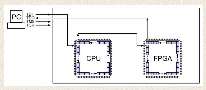
JTAG (Joint Test Action Group) started primarily as a debugging interface for CPLDs or more commonly boundary scan testing, which is explained later. The simplest implementation of the JTAG interface requires 4 signal wires, primarily
- TDO (Test Data Out) – This is output signal from the target in response to the test query.
- TDI (Test Data In) – This is the input signal for the target carrying the test query.
- TCK (Test Clock) – This is the synchronization clock signal
- TMS (Test-Mode Select) – This controls the TAP state, explained later.

Signals Explained
- TCK – is the JTAG clock signal. The other JTAG signals (TDI, TDO, TMS) are synchronous to TCK. So TCK has to toggle for anything to happen (usually things happen on TCK’s rising edge).
- TMS – Inside each JTAG IC, there is a JTAG TAP controller. The TAP controller is mainly a state machine with 16 states. TMS is the signal that controls the TAP controller. The TAP state diagram can be easily found in data-sheets of several JTAG ICs.The little numbers (“0” or “1”) close to each arrow are the value of TMS to change state. So for example, if a TAP controller is at state “Select DR-Scan” and TMS is “0” and TCK toggles, the state changes to “Capture-DR”.
- TDI and TDO – These signals carry the query and its response respectively. Referring to the TAP state diagram, Shift-DR and Shift-IR are the states where the query is generally pushed and Shift-DR is the state where the response is collected.
The TDI and TDO are daisy-chained. That is, with the Shift-DR size equal to 1-bit, data sent through the TDI starts coming back through the TDO after one clock pulse. Hence, when a response is to be collected from Shift-DR, clock pulses are sent to receive the response on the TDO. For example, if the Shift-DR size is 32 bits, 32 pulses are sent to completely receive the response of the JTAG query.
Registers
Each JTAG IC has one instruction register (IR) and multiple data registers (DR). Each instruction to the IR selects a different data register whose value is shifted out as explained above. For example, a 8-bit IR can select up to 256 DR, if available.
The length of each DR and IR registers can be found from the .bsdl file of the specific JTAG IC.
Instructions
The IR registers take in specific intructions which are listed in the .bsdl file of the JTAG IC. The most common of them grabbed from a .bsdl file are
attribute INSTRUCTION_LENGTH of EP1C3T100 : entity is 10;

attribute INSTRUCTION_OPCODE of EP1C3T100 : entity is

  "BYPASS            (1111111111), "&

  "EXTEST            (0000000000), "&

  "SAMPLE            (0000000101), "&

  "IDCODE            (0000000110), "&

  "USERCODE          (0000000111), "&

  "CLAMP             (0000001010), "&

  "HIGHZ             (0000001011), "&

  "CONFIG_IO            (0000001101)";

attribute INSTRUCTION_CAPTURE of EP1C3T100 : entity is "0101010101";

attribute IDCODE_REGISTER of EP1C3T100 : entity is

  "0000"&               --4-bit Version

  "0010000010000001"&   --16-bit Part Number (hex 2081)

  "00001101110"&        --11-bit Manufacturer's Identity

  "1";                  --Mandatory LSB

attribute BOUNDARY_LENGTH of EP1C3T100 : entity is 339;
Querying the JTAG Chain
Whenever the JTAG IC powers up it may end in any TAP state. Hence, it is mandatory to get it to a known state. One such method which is guaranteed to toggle the TAP state to Test-Logic-Reset is to hold TMS high for five clock cycles.
- Set TMS high.
- Send minimum of five clock cycles.
- Set TMS low.
1. Count number of ICs on the JTAG chain
One important IR value is the “all-ones” value. For the CPU that would be 11111 and for the FPGA, that’s 1111111111. This value corresponds to the mandatory IR instruction called BYPASS. In bypass mode, the TAP controller DR register is always a single flip-flop which does nothing besides delaying the TDI input by one clock cycle before outputting to TDO.
One interesting way to use this BYPASS mode is to count the number of ICs that are present in the JTAG chain.
If each JTAG IC delays the TDI-TDO chain by one clock, we can send some data and check by how long it is delayed. That gives us the number of ICs in the chain.
2. Identify ICs on the JTAG Chain
The IDCODE instruction is used to identify ICs on the JTAG chain. The IDCODE instruction is automatically executed once the TAP state is forced to Test-Logic-Reset i.e the IDCODE data register appears on the TDO line. It is usually 32-bits long.
- Go to Test-Logic-Reset.
- Go to Shift-DR.
- Shift out 32 bits of data onto the TDO line by passing 32 clock pulses. LSB comes out first.
Similarly, other instruction can be passed to the IR and response read from the Shift-DR TAP state.
Boundary Scan Testing
This was the primary purpose of the JTAG interface when it was launched. In the boundary scan mode, the DR chain goes through each IO block and can read or hijack each pin.
Boundary-scan can be used even while a device is otherwise running. So for example, using JTAG on an FPGA, you can tell the status of each pin while the FPGA is running. The SAMPLE instruction is used in running a boundary scan. The .bsdl file lists the size of the boundary scan chain and the various pad configurations. In the .bsdl above, the length is 339 bits listed in the last line. Each pin use an IO pad on the IC die. Some IO pads use one, two or three bits from the chain (depending if the pin is input only, output with tri-state, or both). Also some registers correspond to IO pads that may not be bounded (they exists on the IC die but are not accessible externally). Which explains why a 100 pins device can have a 339 bits boundary-scan chain.
attribute BOUNDARY_REGISTER of EP1C3T100 : entity is

  --BSC group 0 for I/O pin 100

  "0   (BC_1, IO100, input, X)," &

  "1   (BC_1, *, control, 1)," &

  "2   (BC_1, IO100, output3, X, 1, 1, Z)," &

  --BSC group 1 for I/O pin 99

  "3   (BC_1, IO99, input, X)," &

  "4   (BC_1, *, control, 1)," &

  "5   (BC_1, IO99, output3, X, 4, 1, Z)," &

  ...

  ...

  ...

  --BSC group 112 for I/O pin 1

  "336 (BC_1, IO1, input, X)," &

  "337 (BC_1, *, control, 1)," &

  "338 (BC_1, IO1, output3, X, 337, 1, Z)" ;
This lists all the 339 bits of the chain, and what they do.
For example, bit 3 is the one that tells us what is the value on pin 99.
Querying the boundary scan chain is straightforward.
- Go to Shift-IR state.
- Shift in SAMPLE instruction with TMS low.
- Go to Exit1-IR.
- Go to Shift-DR.
- In our case, the data register is 339 bits long, Read the contents of the Shift-DR over TDO by sending 339 clock pulses with TMS low.
Using the JTAG interface, is pretty simple. It is basically a serial interface with a ‘cool’ name. You shift out a query and shift in the response. Knowledge of this interface is essential as its use is increasing day by day. Almost every microprocessor now uses it as a primary hardware debugging interface.
JTAG Simplified的更多相关文章
- JTAG 引脚自动识别 JTAG Finder, JTAG Pinout Tool, JTAG Pin Finder, JTAG pinout detector, JTAGULATOR, Easy-JTAG, JTAG Enumeration
JTAG Finder Figuring out the JTAG Pinouts on a Device is usually the most time-consuming and frustra ...
- SWD and JTAG selection mechanism
SWD and JTAG selection mechanism SWJ-DP enables either an SWD or JTAG protocol to be used on the deb ...
- Design Patterns Simplified - Part 3 (Simple Factory)【设计模式简述--第三部分(简单工厂)】
原文链接:http://www.c-sharpcorner.com/UploadFile/19b1bd/design-patterns-simplified-part3-factory/ Design ...
- STM32C8T6 JTAG使用到PB3|PB4|PA13|PA14|PB15端口做普通IO时,需禁止JTAG!
GPIO_InitTypeDef GPIO_InitStructure; RCC_APB2PeriphClockCmd(RCC_APB2Periph_GPIOB|RCC_APB2Periph_GPIO ...
- STM32用JLINK 烧写程序时出现NO Cortex-m device found in JTAG chain现象和解决方案
现象 CPU: STM32107VC 用JLINK 烧写程序时出现NO Cortex-m device found in JTAG chain 如图无法查找到硬件就是CPU 提示1:NO Cortex ...
- 偶遇STM32 JTAG和SWD口(调试)被禁用无法下载,已经粗暴解决!
处女座,为了板子走线美观,拉线方便,在项目量产前,还更改了原来外设的IO口,埋头苦干一天,移植ok,发现PB3一直不听使唤,好,加班检查代码,检查初始化,时钟,IO对应,然后试PCB板,是否短路,断路 ...
- Design Patterns Simplified - Part 2 (Singleton)【设计模式简述--第二部分(单例模式)】
原文链接: http://www.c-sharpcorner.com/UploadFile/19b1bd/design-patterns-simplified-part-2-singleton/ De ...
- 【翻译】设计模式学习系列1---【Design Patterns Simplified: Part 1【设计模式简述:第一部分】】
原文链接:http://www.c-sharpcorner.com/UploadFile/19b1bd/design-patterns-simplified-part1/ Design Pattern ...
- (转)小心FPGA的JTAG口(上电和下电顺序)
同志们,根据ALTERA官方FAE(现场应用工程师)的强烈建议,请注意不要随意带电插拔你的JTAG下载接口,否则会损坏FPGA芯片的JTAG口信号管脚.现象:在排除了下载线的问题后,还是不能访问FPG ...
随机推荐
- linux设备驱动归纳总结(三):3面向对象思想和lseek、container_of、write、read 【转】
linux设备驱动归纳总结(三):3.设备驱动面向对象思想和lseek的实现 转自:http://blog.chinaunix.net/uid-25014876-id-59418.html 一.结构体 ...
- 008_MAC 终端使用技巧
一.常用终端命令. <1>reset 的作用很简单——将目前「终端」屏幕上的内容清空,就好像刚刚打开终端一样. <2>如果你在一条终端命令中发现有输入错误的话,那么用 cont ...
- 2013 ACM/ICPC 杭州网络赛C题
题意:驴和老虎,在一个矩阵的两个格子里,有各自的起始方向.两者以相同的速度向前移动,前方不能走时驴总是向右,老虎总是向左.他们不能超出矩阵边界也不能走自己走过的格子(但可以走对方走过的格子).如果不能 ...
- ssh隐藏的sftp功能的使用
sftp是Secure File Transfer Protocol的缩写,安全文件传送协议.可以为传输文件提供一种安全的加密方法.sftp 与 ftp 有着几乎一样的语法和功能.SFTP 为 SSH ...
- java 内部类和向上转型
当将内部类向上转型为其基类时,尤其是转型为一个接口的时候,内部类就有了用武之地,(从实现某个接口的对象,得到对接口的引用,与向上转型为这个对象的基类,实际上是一样的效果,),这是因为此内部类---某个 ...
- *使用配置类定义Codeigniter全局变量
之前提到的 CodeIgniter 引入自定义公共函数 这篇文章提到了公共函数实现,全局的变量也可以借助 helper 函数来实现.不过,更为合适的方式可能要属用配置类定义了. CodeIgniter ...
- IntelliJ IDEA 设置Output 窗口字体大小
Settings——>Editor——>Colors&Fonts——>Console Font 如图: 字体调好了以后使用起来眼睛就轻松多了
- Java第三阶段学习(九、类加载器、反射)
一.类加载器 1.类的加载: 当程序要使用某个类时,如果该类还未被加载到内存中,则系统会通过加载,连接,初始化三步来实现对这个类进行初始化. 1.1 加载: 就是指将class文件读入内存,并为之自动 ...
- pig cookbook学习
pig cookbook学习 Overview 近期需要用pig做一些统计,由于没有系统学习,问题出现一些问题,且不容易调试,执行效率也不高.所以打算看一些官方文档,在此做些笔记. pig性能提升 指 ...
- Boost学习资源
http://blog.csdn.net/huang_xw/article/details/8758212