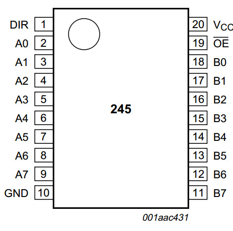
74HC245 74HCT245 74LV245 74LVC245 74LVC4245A 74LVC8T245 74LVC16T245 74ALVC164245
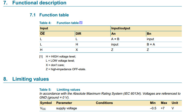
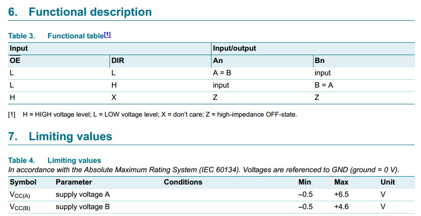
OE controls the outputs so that the buses are effectively isolated.
The 74HC245; 74HCT245 is similar to the 74HC640;
74HCT640 but has true (non-inverting) outputs.
■ Octal
2024-10-13 17:37:53 原文74HC245/74HCT245
The 74HC245; 74HCT245 is a high-speed Si-gate CMOS device and is
pin compatible with Low-Power Schottky TTL (LSTTL).
The 74HC245; 74HCT245 is an octal transceiver featuring non-inverting 3-state bus
compatible outputs in both send and receive directions.
The 74HC245; 74HCT245 features an output enable input (OE) for easy cascading
and a send/receive input (DIR) for direction control.
OE controls the outputs so that the buses are effectively isolated.
The 74HC245; 74HCT245 is similar to the 74HC640;
74HCT640 but has true (non-inverting) outputs.
■ Octal bidirectional bus interface
■ Non-inverting 3-state outputs
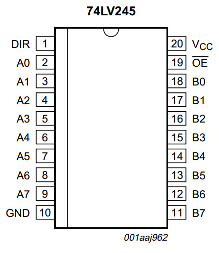
74LV245
Octal bus transceiver (3-State)
The 74LV245 is a low-voltage Si-gate CMOS device that is pin
and function compatible with 74HC245 and 74HCT245.
The 74LV245 is an octal transceiver with non-inverting 3-state bus
compatible outputs in both send and receive directions.
A send/receive (DIR) input controls direction, and an output enable (OE)
input makes easy cascading possible.
Pin OE controls the outputs so that the buses are effectively isolated.
Wide operating voltage: 1.0 V to 5.5 V
Optimized for low voltage applications: 1.0 V to 3.6 V
Accepts TTL input levels between VCC = 2.7 V and VCC = 3.6 V
Typical output ground bounce < 0.8 V at VCC = 3.3 V and Tamb = 25 °C
Typical HIGH-level output voltage (VOH) undershoot: > 2 V at VCC = 3.3 V and Tamb = 25 °C
74LV245A
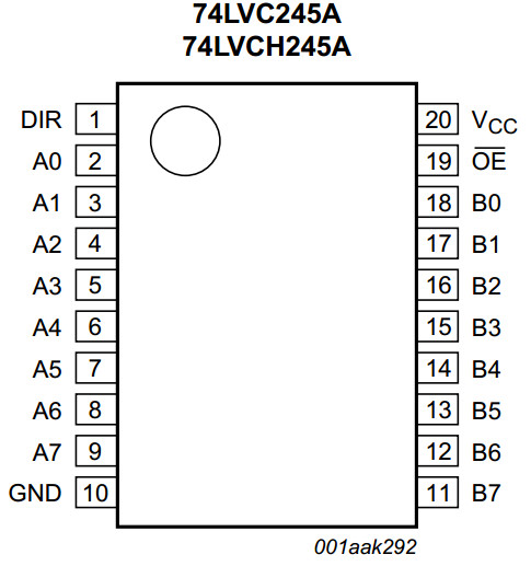
The 74LVC245A; 74LVCH245A are 8-bit transceivers featuring non-inverting 3-state bus
compatible outputs in both send and receive directions.
The device features an output enable (OE) input for easy cascading and
a send/receive (DIR) input for direction control.
OE controls the outputs so that the buses are effectively isolated.
Inputs can be driven from either 3.3 V or 5 V devices.
When disabled, up to 5.5 V can be applied to the outputs.
These features allow the use of these devices in mixed 3.3 V and 5 V applications.
The 74LVCH245A bus hold on data inputs eliminates the need for external pull-up
resistors to hold unused inputs.
5 V tolerant inputs/outputs for interfacing with 5 V logic
Wide supply voltage range from 1.2 V to 3.6 V
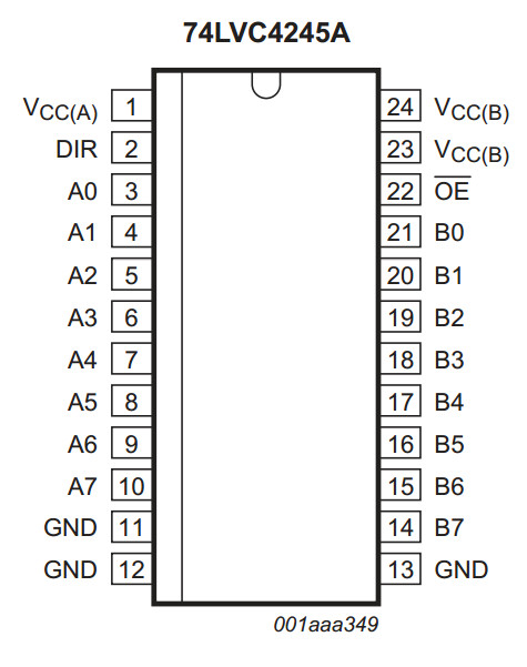
74LVC4245A
Octal dual supply translating transceiver; 3-state
The 74LVC4245A is an octal dual supply translating transceiver featuring
non-inverting 3-state bus compatible outputs in both send and receive directions.
It is designed to interface between a 3 V and 5 V bus
in a mixed 3 V and 5 V supply environment.
The device features an output enable input (pin OE) for
easy cascading and a send/receive input (pin DIR) for direction control.
Pin OE controls the outputs so that the buses are effectively isolated.
In suspend mode, when VCC(A) is zero, there will be
no current flow from one supply to the other supply.
The A-outputs must be set 3-state and the voltage on the A-bus
must be smaller than Vdiode (typical 0.7 V).
VCC(A) >= VCC(B), except in suspend mode.
5 V tolerant inputs/outputs, for interfacing with 5 V logic
Wide supply voltage range:
3 V bus (VCC(B)): 1.5 V to 3.6 V
5 V bus (VCC(A)): 1.5 V to 5.5 V
CMOS low-power consumption
Direct interface with TTL levels
Inputs accept voltages up to 5.5 V
High-impedance when VCC(A) = 0 V
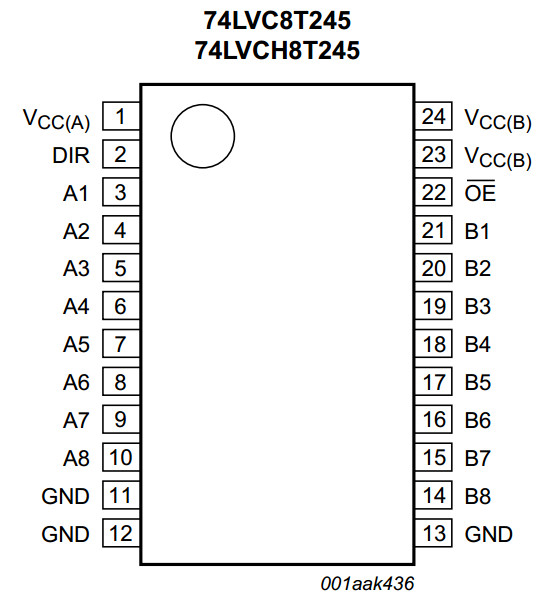
74LVC8T245
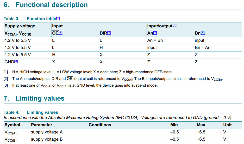
The 74LVC8T245; 74LVCH8T245 are 8-bit dual supply translating transceivers
with 3-state outputs that enable bidirectional level translation.
They feature two data input-output ports (pins An and Bn), a direction control input (DIR),
an output enable input (OE) and dual supply pins (VCC(A) and VCC(B)).
Both VCC(A) and VCC(B) can be supplied at any voltage between 1.2 V and 5.5 V
making the device suitable for translating between any of the low voltage nodes
(1.2 V, 1.5 V, 1.8 V, 2.5 V, 3.3 V and 5.0 V).
Pins An, OE and DIR are referenced to VCC(A) and pins Bn are referenced to VCC(B).
A HIGH on DIR allows transmission from An to Bn and
a LOW on DIR allows transmission from Bn to An.
The output enable input (OE) can be used to disable the outputs
so the buses are effectively isolated.
The devices are fully specified for partial power-down applications using IOFF.
The IOFF circuitry disables the output, preventing any damaging backflow current
through the device when it is powered down.
In suspend mode when either VCC(A) or VCC(B) are at GND level,
both A port and B port are in the high-impedance OFF-state.
Active bus hold circuitry in the 74LVCH8T245 holds unused or
floating data inputs at a valid logic level.
Wide supply voltage range:
VCC(A): 1.2 V to 5.5 V
VCC(B): 1.2 V to 5.5 V
74LVC16T245
- Control Inputs VIH/VIL Levels Are Referenced to VCCA Voltage
- VCC Isolation Feature - If Either VCC Input Is at GND,
Both Ports Are in the High-Impedance State - Overvoltage-Tolerant Inputs/Outputs Allow Mixed-Voltage-Mode Data Communications
- Fully Configurable Dual-Rail Design Allows Each Port
to Operate Over the Full 1.65-V to 5.5-V Power-Supply Range
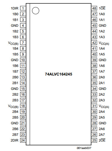
74ALVC164245
16-bit dual supply translating transceiver; 3-state
The 74ALVC164245 is a high-performance, low-power, low-voltage, Si-gate CMOS
device, superior to most advanced CMOS compatible TTL families.
The 74ALVC164245 is a 16-bit (dual octal) dual supply translating transceiver featuring
non-inverting 3-state bus compatible outputs in both send and receive directions. It is
designed to interface between a 3 V and 5 V bus in a mixed 3 V and 5 V supply
environment.
This device can be used as two 8-bit transceivers or one 16-bit transceiver.
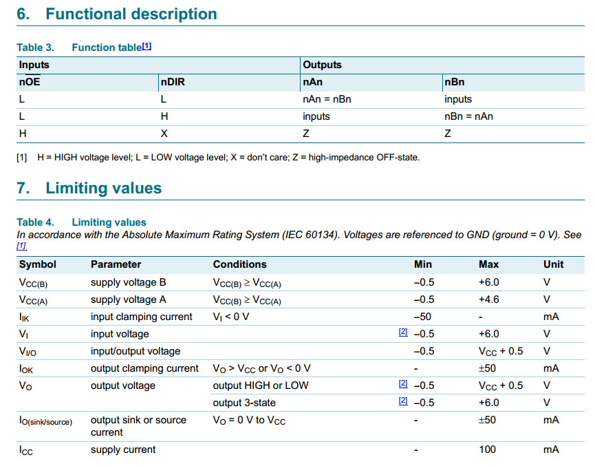
The direction control inputs (1DIR and 2DIR) determine the direction of the data flow.
nDIR (active HIGH) enables data from nAn ports to nBn ports. nDIR (active LOW) enables
data from nBn ports to nAn ports. The output enable inputs (1OE and 2OE), when HIGH,
disable both nAn and nBn ports by placing them in a high-impedance OFF-state. Pins
nAn, nOE and nDIR are referenced to VCC(A) and pins nBn are referenced to VCC(B).
In suspend mode, when one of the supply voltages is zero, there will be no current flow
from the non-zero supply towards the zero supply. The nAn-outputs must be set 3-state
and the voltage on the A-bus must be smaller than Vdiode (typical 0.7 V). VCC(B) VCC(A)
(except in suspend mode).
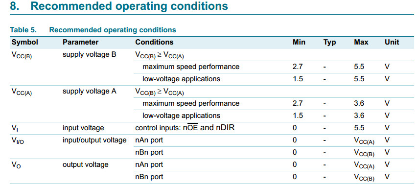
5 V tolerant inputs/outputs for interfacing with 5 V logic
Wide supply voltage range:
3 V port (VCC(A)): 1.5 V to 3.6 V
5 V port (VCC(B)): 1.5 V to 5.5 V
CMOS low power consumption
Direct interface with TTL levels
Control inputs voltage range from 2.7 V to 5.5 V
Inputs accept voltages up to 5.5 V
High-impedance outputs when VCC(A) or VCC(B) = 0 V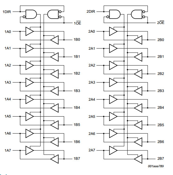
74HC245 74HCT245 74LV245 74LVC245 74LVC4245A 74LVC8T245 74LVC16T245 74ALVC164245的更多相关文章
- 74HC245引脚定义 使用方法
典型的CMOS型三态缓冲门电路,八路信号收发器. 由于单片机或CPU的数据/地址/控制总线端口都有一定的负载能力,如果负载超过其负载能力,一般应加驱动器. 主要应用于大屏显示 引脚定义 DIR:方向控 ...
- 5V系统和3.3V系统电平转换
在设计一个带MCU或者ARM系统电路时候,经常遇见MCU的VCC是3.3V,但是外围电路需要5V.有时候是反过来.虽然现在MCU的IO都声称支持TTL电平,但是我们谁也不想将MCU的IO口直接接上5V ...
- AC、HC、AHC、ACT、LS的区别
http://forum.eet-cn.com/thread!printPreview.jspa?threadID=1200029698&start=0 以245为例,74AC245.74HC ...
- MSP430常见问题之LCD 显示驱动类
Q1:晶体一般都是接32768,然后使用液晶很正常.我打算将晶体接6M的替换32768,那么液晶还能正常显示吗A1:看你所用的LCM 模块时序极限是多少HZ,然后看6M情况下,MSP430去驱动LCM ...
- IC芯片
5.8寸显示屏/LB058WQ1(SD)01LG2 74HC04 0.3NXP10K 74HC138 0.37NXP20K 74HC245 0.52NXP30K 74HC595 明威 ...
- 初识DSP
初识DSP 1.TI DSP的选型主要考虑处理速度.功耗.程序存储器和数据存储器的容量.片内的资源,如定时器的数量.I/O口数量.中断数量.DMA通道数等.DSP的主要供应商有TI,ADI,Motor ...
- 基于Verilog HDL 的数字时钟设计
基于Verilog HDL的数字时钟设计 一.实验内容: 利用FPGA实现数字时钟设计,附带秒表功能及时间设置功能.时间设置由开关S1和S2控制,分别是增和减.开关S3是模式选择:0是正常时钟 ...
- 豹哥嵌入式好讲堂:ARM Cortex-M调试过程探析(1)- 4线接口标准(JTAG)
大家好,我是豹哥,猎豹的豹,犀利哥的哥.今天豹哥给大家讲的是嵌入式调试里的接口标准JTAG. 在结束<ARM Cortex-M开发文件详解>系列文章之后,豹哥修整了一小段时间,但是讲课的心 ...
- 学习笔记——单片机简介 & 点亮LED & 流水灯 & 电路基础【更新Ing】
视频地址:https://www.bilibili.com/video/av10765766 超详细!!!!!! 单片机内部三大资源 [资源:单片机可提供使用的东西] FLASH 可以重复擦写 断电后 ...
随机推荐
- 【前端】h5音乐播放demo 可关闭可播放
复制如下代码,直接可预览(记得把超链接换成自己本地路径) <!DOCTYPE html> <html> <head> <meta charset=" ...
- CF 983B 序列函数
CF 983B 序列函数 一道本校神仙wucstdio出的毒瘤签到题. 题意: 给你一段序列,求出它们的最大异或和. 解法: 其实这道题并不很难,但读题上可能会有困难. 其实样例我是用Python 3 ...
- JQ + CSS实现浪漫表白必备
JQ + CSS实现浪漫表白必备页面 效果图: 图片素材 : 代码如下,复制即可使用: <!DOCTYPE html> <html> <head> <meta ...
- SQLServer 查看备份进度
SELECT DB_NAME(er.[database_id]) [DatabaseName], er.[command] AS [CommandType], er.[percent_comp ...
- 关于URL编码(针对URL含有中文的参数)
http://www.ruanyifeng.com/blog/2010/02/url_encoding.html 一.问题的由来 URL就是网址,只要上网,就一定会用到. 一般来说,URL只能使用英文 ...
- JavaScript工程师都应懂的33个概念
最近福利发的有点多啊,各种硬干货,小伙伴们是不是觉得很爽啊.Github真的蕴含着各种各样的宝藏,难怪各个大厂也都纷纷贡献自己的代码到Github上. 所以各种干货还是会源源不断的po给大家,觉得有帮 ...
- Bad connection to FS. command aborted. exception: Call to chaoren/192.168.80.100:9000 failed on connection exception: java.net.ConnectException: Connection refused
Bad connection to FS. command aborted. exception: Call to chaoren/192.168.80.100:9000 failed on conn ...
- Django 学习总结(更新中)
1.常用命令 新建一个项目:django-admin.py startproject project-name 新建一个app:python manage.py startapp app-name 同 ...
- DDR3调试记录
FPGA采集视频数据并写到DDR3,然后从DDR3读出并送给显示终端显示.不能稳定显示.但用FPGA内部逻辑产生color bar写到DDR3后读出来显示正常.因此DDR3部分逻辑没有问题 ...
- vue 单向数据流 & 双向绑定
在react中是单向数据绑定,而在vue中的特色是双向数据绑定.但是其实就我个人的理解是: 其实无论是vue还是react其实还是提倡单向数据流去管理状态,这一点在vuex和redux状态管理器上体现 ...