Open Source Universal 48 pin programmer design
http://www.edaboard.com/thread227388.html
Hi, i have designed a 48 pin universal programmer but need help finishing it off, is anyone up for the challange?
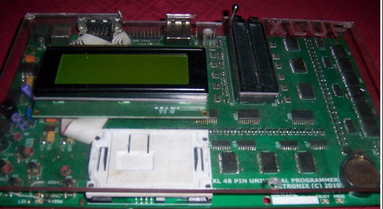
Programmer info:
LPC2388 ARM7TDMI CPU with USB
2XDC/DC Converters
48 universal pin drivers which can be either GND/VCC/VPP/HI,LO/CLOCK/INPUT
Smart card interface
ISP socket which is used for JTag for FPGA's/CPLD/ARMs Anything JTag... /serial programming devices mounted on a board Pic's/AVR's etc/In car Dashboards/ECU's etc
USB Interface
Ethernet Interface
SD card
LCD
Serial interface
Buttons/switches lights etc
JTAG For ARM
JTAG for FPGA
Soft JTAG for FPGA
This is really a massive project and has taken me a while to get this far, i think i need help to finish it.
The software is written in delphi:

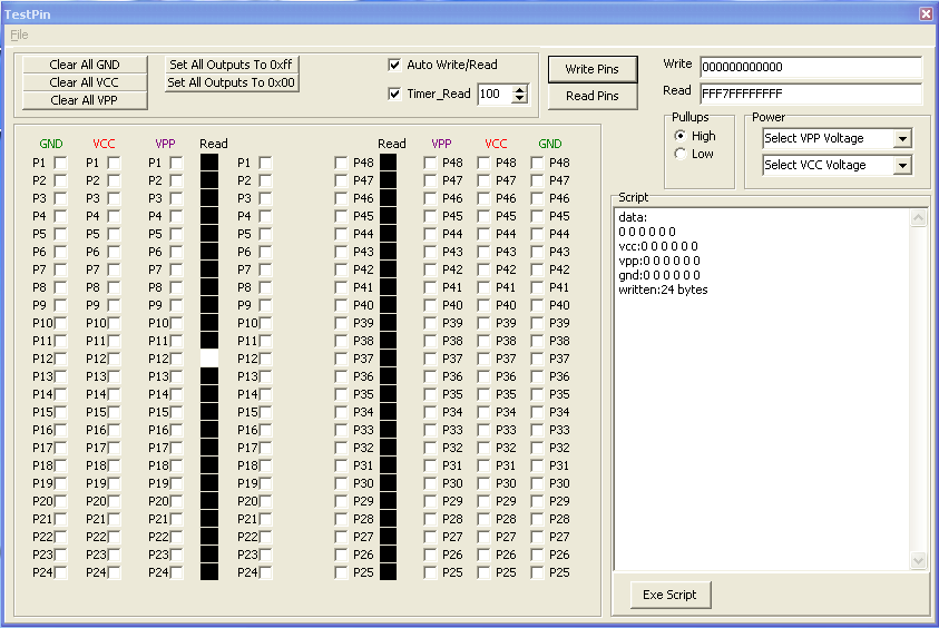
USB Uses CDC So can be used on any PC.
So far i can read and write to all pins fine, program the FPGA, etc
There are three parts to the programmer.
Firmware:
Written in C using Keil compiler.
FPGA:
Designs are done in Altium.
PC Software:
Written in Delphi 7
I am very good with the firmware, and not bad with the FPGA, the PC software is not good for me...
I want the software, fpga designs and the firmware to be OPEN SOURCE, this was the idea behind it, as you cannot by a good true universal programmer for less than around £500 i thought it would be a good project to undertake, with the added benefit of a smart card programmer and ISP it should be a good device, and hoping to ship it for less than £100
So if you are up for a challange let me know......
Many Thanks....
Picman....
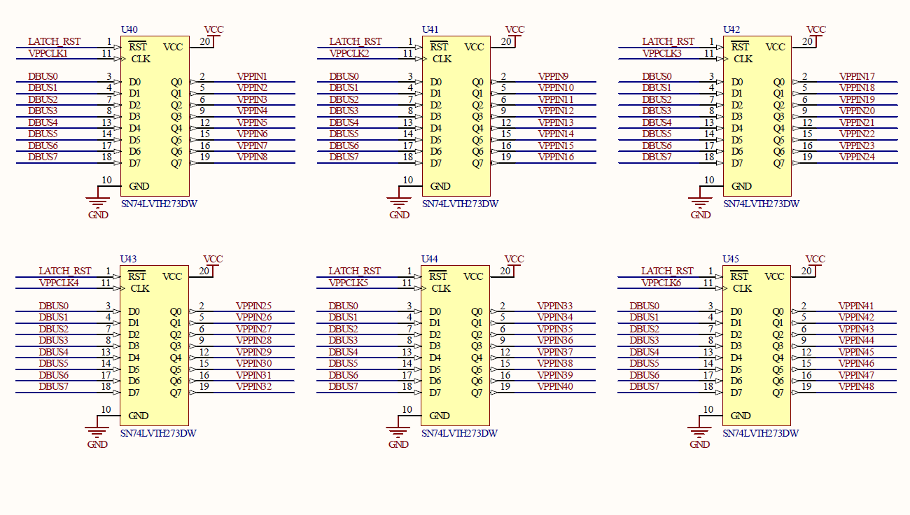
Programmer Schematics....
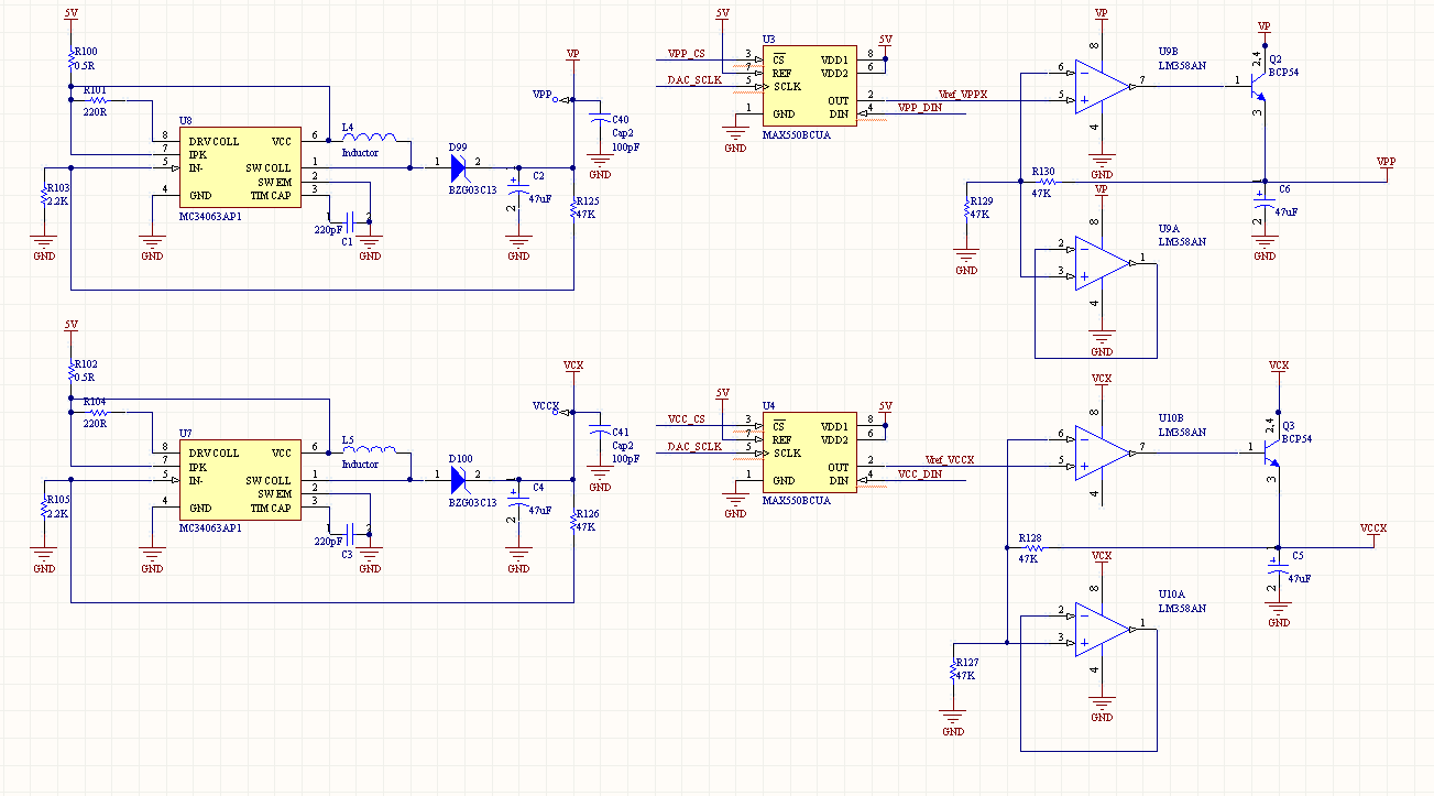
The PSU for VCC and VPP need changing does not work too well, but i think it would be good to only need the 5V from the USB to power the programmer, so DC/DC converters are needed to get VPP.
The FPGA is key to the programmers functionallity, even if you just use it to route pins to the micro so using it as a pin matrix. but you can do a lot more with it there, as it is, it will program most programmable devices on the market.
I am fine with coding the verilog for the fpga anyway..
What about replacing fpga with cpld? You can get those in packages like qfp44. This would somewhat reduce difficulty of assemblying it at home.
Unfortunately there are 48 IO's from the ziff so it needs a larger package than the 44 pin, i have assembled 2 of these at home an both work fine, just takes a little time. also the ARM is 144 pins and most pins are used.
Anyway the basic idea will be to sell the boards already made, but open source the software, but i do see where you are comming from for the development.
Having 200K gates also opens up a lot more potential for doing some clever things in the fpga, and freeing the CPU from a lot of tasks. For instance a logic analyzer.....
If idea is to sell the board already made than large footprint FPGA is fine.
A logic analyzer is also a nice idea, but for it to have good parameters you need an external RAM chip, because the bandwidth of USB is insufficient for analyzing high speed signals.
I think that it would be nice if your device was able to switch between different compatibility mode. I mean that you could set it up to work like pickit 2 and be able to use it from MPLAB. Or set it up to work like STK500 and be able to use it from AVR studio. That would increase functionality creatly, because most people find it far more convenient to be able to operate programmer/debugger straight from IDE.
I realize that it would need enormous amount of coding and reverse engineering, but having a universal programmer with IDE compatibility would be very nice.
What would you use the IDE for? If its programming the ARM then there is already an IDE which i use called KEIL.
No, I mean the IDE which u will be using to develop software that you will later download into some device using this programmer. Or maybe I got the purpose of this device wrong?
To achieve 48 pin drive all, the fpga haved more than 48 io's and Dynamic reconfiguration
Firmware must be prepared to understand the hardware architecture, and sometimes have to modify the hardware design to suit the software development
I do not know the hardware architecture in the case, there is no other thing that programmers can do
If you want to do open source, then this is a must. If you do the programmer development platform is to provide a schematic
my development :
windows 2003
keil 8.16a
visual c++ 6
Yes a Schematic will be provided, also the interface from the ARM to the FPGA is fixed, so its always the same no matter what device you program.
The purpose of the Programmers is a IC device programmer, like Datamans Dataman 48UXP Universal Programmer
But it can do more because it has a smart card slot, and an ISP plug and also can use ethernet and usb and serial, plus loads more....
It can also be used as a JTAG programmer/debugger etc....
the Programmer‘s vccx and vpp do what needs to be improved
and head3 ,How to use it? do Hand?
Pullups/pulldowns work ok, VCC and VPP need to be redesigned, im not happy with them at the moment.
Whats Head3?
The power supply for vcc and vpp will be controlled by the ARM so we need some digital 3v3 way of changing the voltages on vcc and vpp.
Pullups/pulldowns work ok, VCC and VPP need to be redesigned, im not happy with them at the moment.
Whats Head3?
The power supply for vcc and vpp will be controlled by the ARM so we need some digital 3v3 way of changing the voltages on vcc and vpp.
Ok what voltages can you get on vcc and vpp, what sort of range.. 0..25V and 0..5V???
And what Current?
Do you think it would work fine from 5V from USB?
If so your idea is good...
On the LPC2388 the ARM CPU we only have one DAC, so we would need an external DAC IC for your PSU to work.
Also in you PSU design what about pin 4 on the MC34063? I thought pin 4 was GND and pin 6 was VCC?????
A:
1.
vcp‘s range 1.8~6.8v
vpp’s range 1.8~25V
one step 0.1v
2.By sampling the voltage difference across the resistor to convert current
Programmable reference source and a comparator for protection
Of course, access to and control of current through the operation
3.34063
Use the datasheet of the design
I use the package who have‘nt 6 pin and 4 pin
pin4 gnd
pin6 vcc
Q?Pullups / pulldowns
How it’s work
What is the function in the end
thanks
Pullups are uses as a logic 1.
So to write a 1 to the device being programmed you set the IO pin on the FPGA as HIZ or input, this will allow the Weak pullups to pull the pin to VCCX so putting a logic 1 on the pin.
The point of this is that a logic 1 is always the same as VCCX so if you want to program for example a 2.5V device then as long as VCCX is at 2.5V then the logic 1 will be the same voltage.
If we used the FPGA pin to output a 1 then this would be 3.3v, not good for a 2.5V or 5V or 1.8V device...
Do you understand now?
vcp‘s range 1.8~6.8v
vpp’s range 1.8~25V
one step 0.1v
This sound fine, how many steps has the DAC got?
I think an 8 bit DAC would do fine with 256 steps, 0.2v steps..
I don't think that any IC is that fussy that it needs a resolution better than 0.2V for programming.
So i have found some DACs from Maxim MAX550B that are 8 bit and use a simple SPI serial interface. 8 pin and are 2.5V to 5.5V single supply.
They are also very cheap...
So the new diagram for the PSU would be...
thanks
my programmer‘s vcp is the target chip power supply
Programmable control, can achieve any voltage 1.8 to 6.5v
Q?
Test pin is bad how to achieve it
Test pin is bad how to achieve it ? I don't understand...
Test pin contact is good
Whether short or damage the chip
The chip is inserted upside
These are supported by professional programmers
There voltage rise-time control or increased steepness
??????
I think and think, but did not know there are many
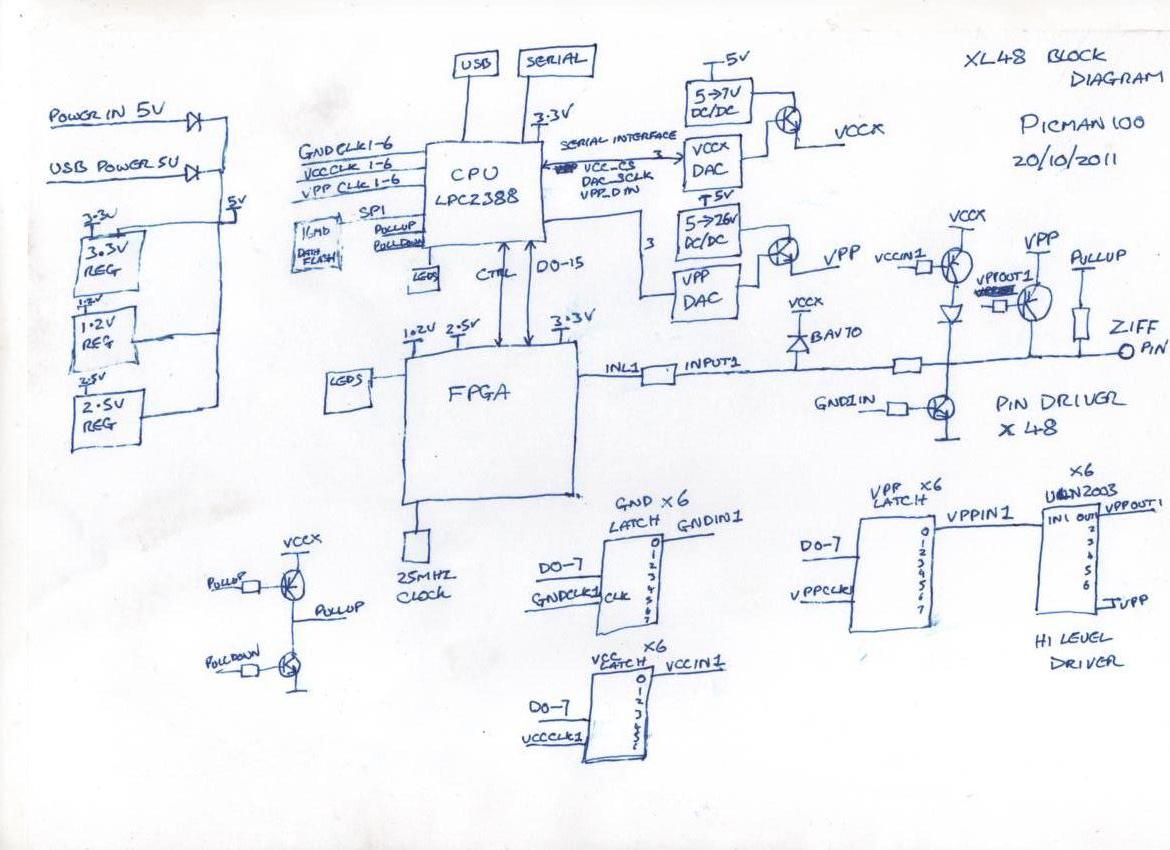
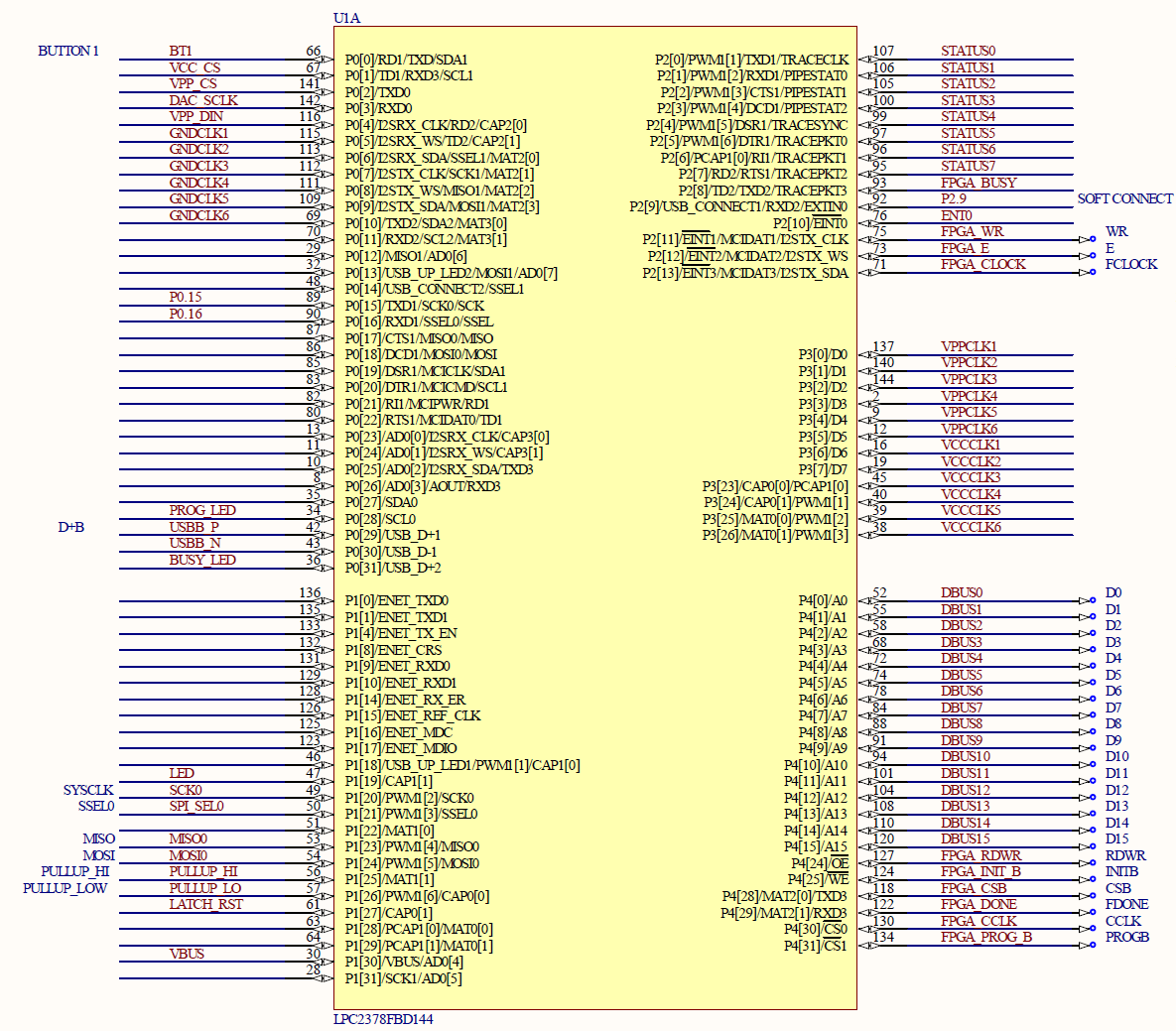
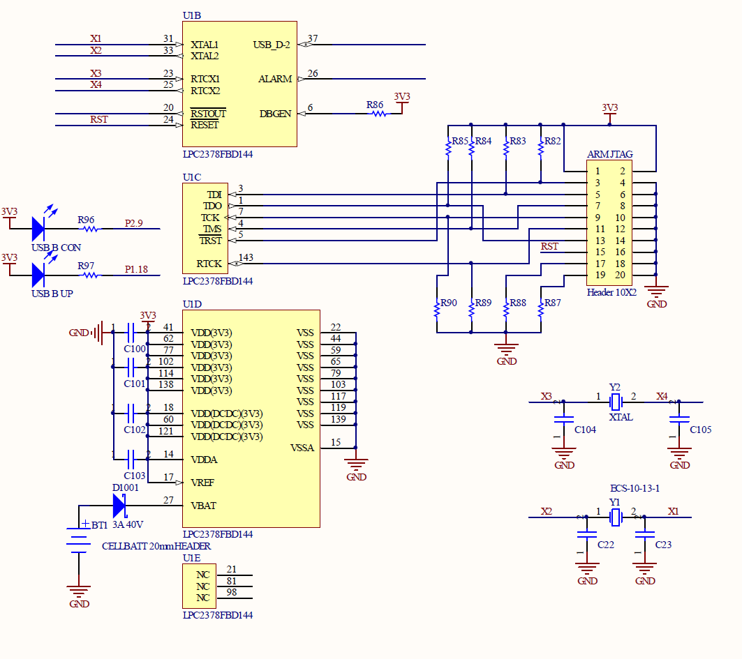
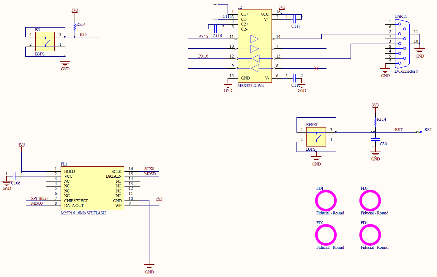
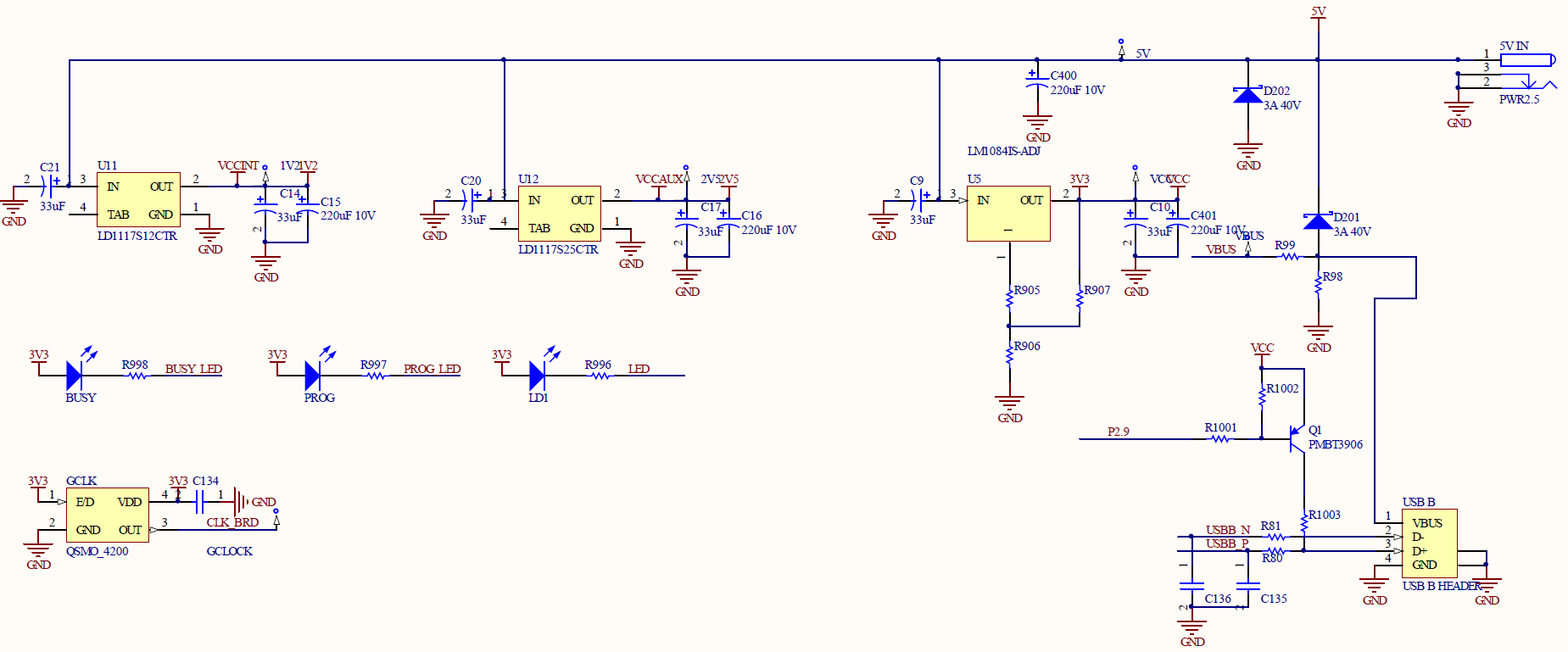
New Schematics
Changes:
DAC controlled PSU for VCCX
DAC controlled PSU for VPP
Ethernet and SDCARD removed.
Smartcard Removed.
LEDs added for status on ARM
LEDs added for status on FPGA.
This should make the programmer cheaper but still function the same.
Take a look at the schematics and tell me what you think.
Programmer supports sd card run offline is a good choice
Dot-lcd display would be better
My idea, please refer to

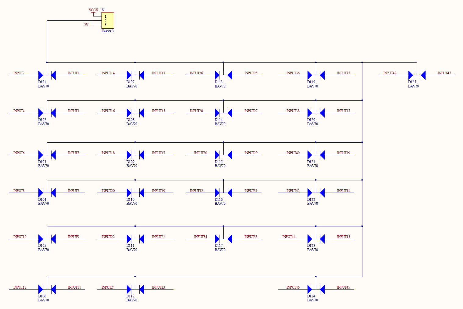
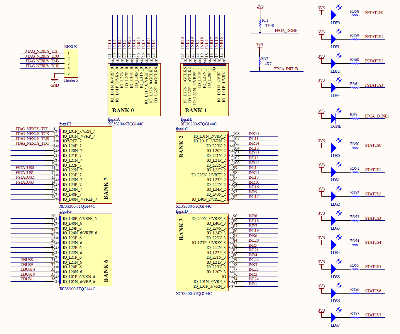
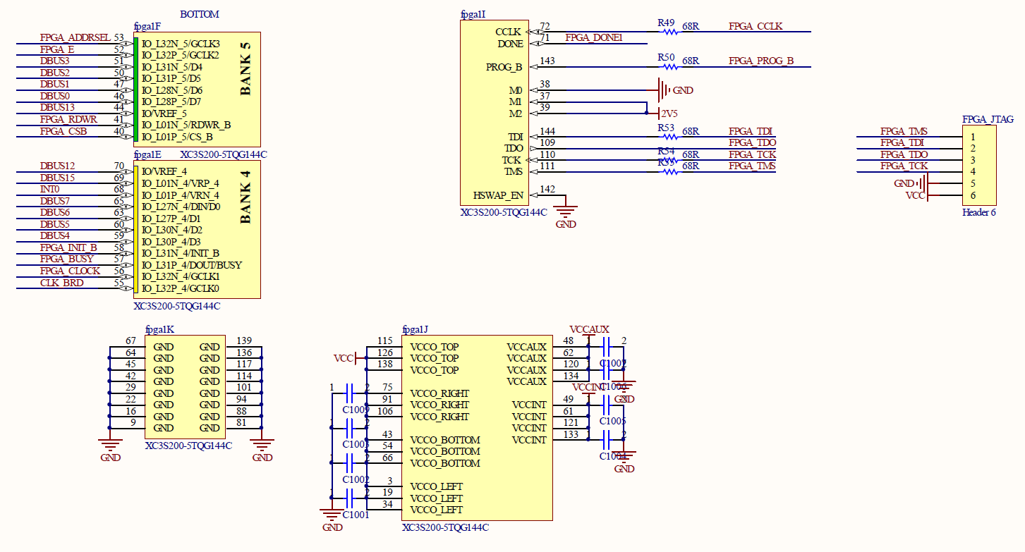
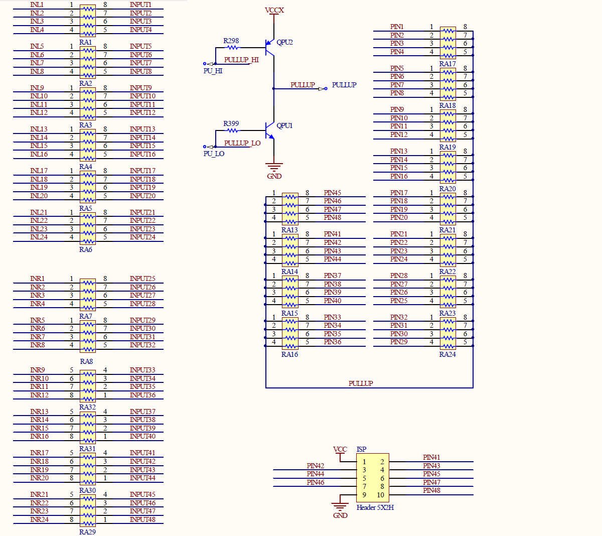
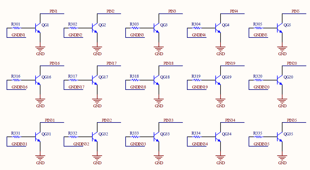
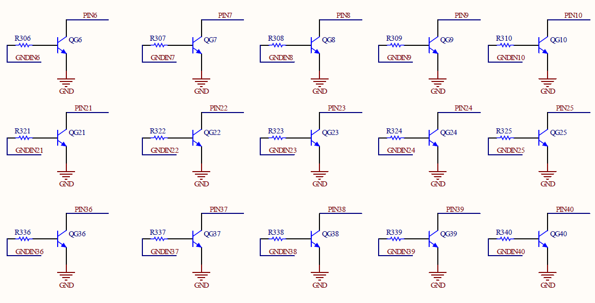
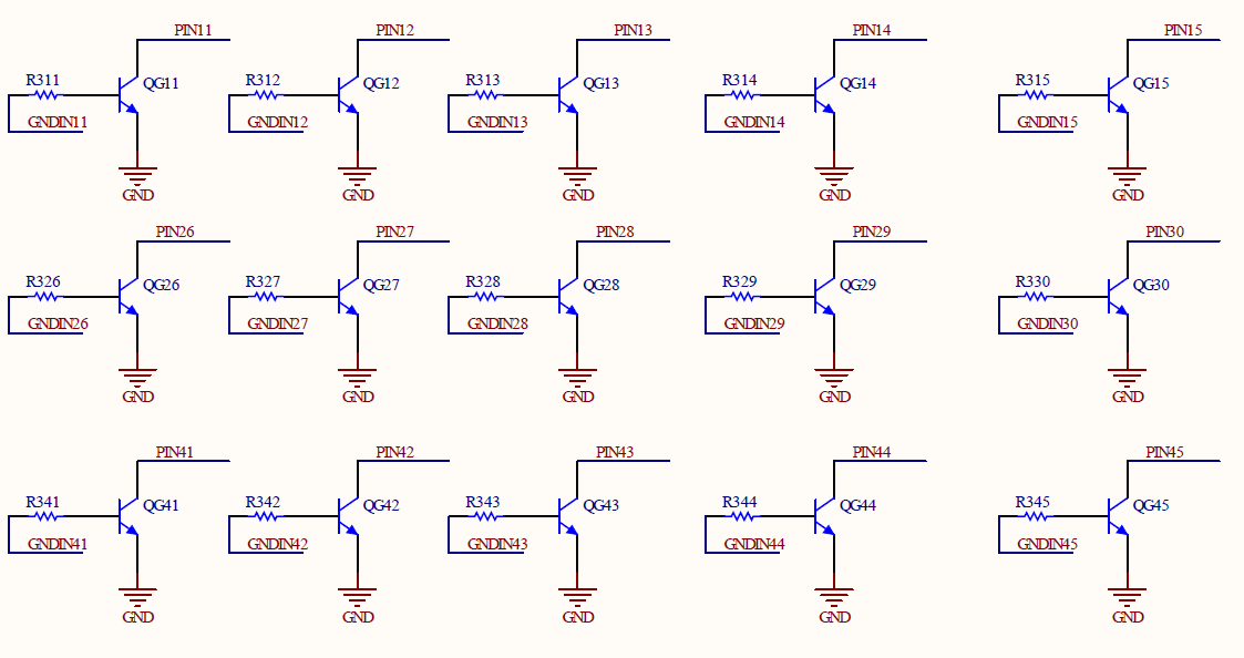
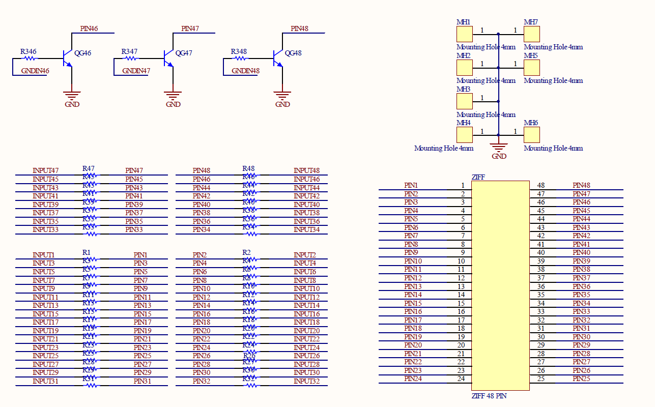
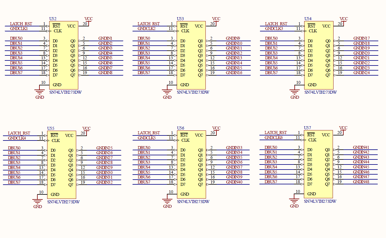
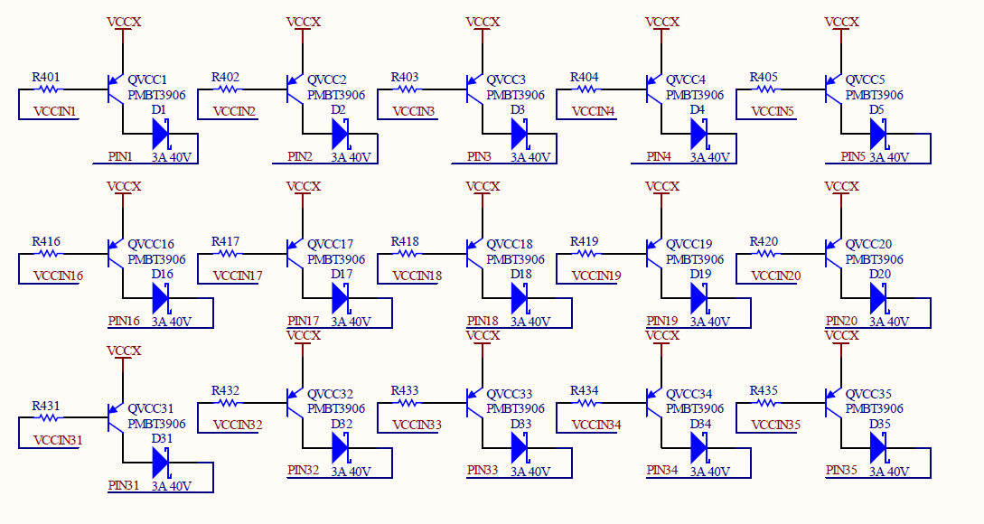

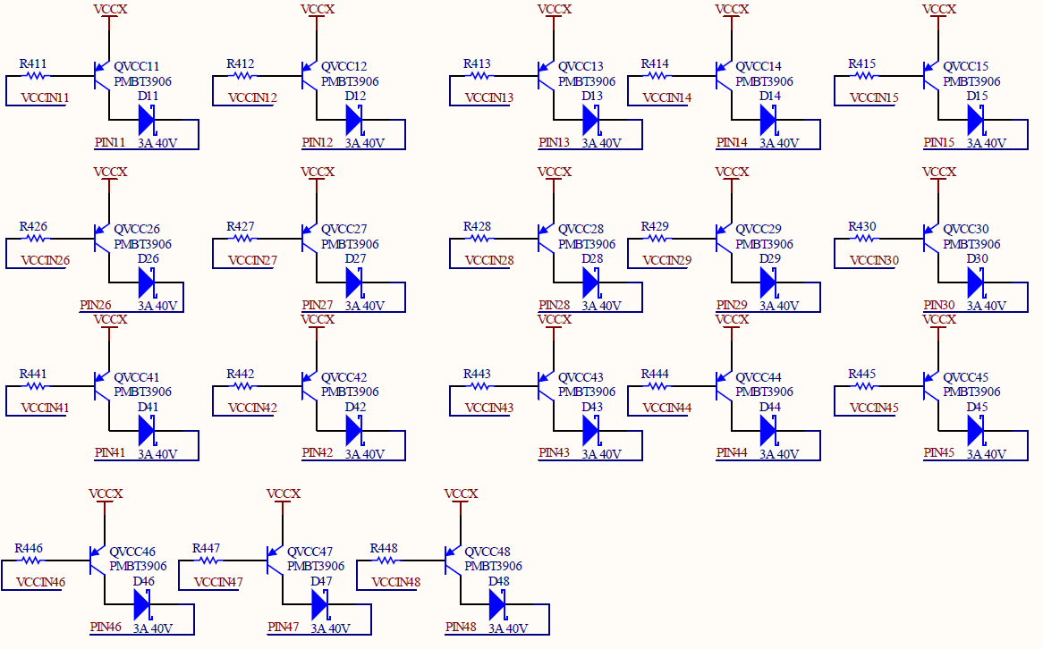
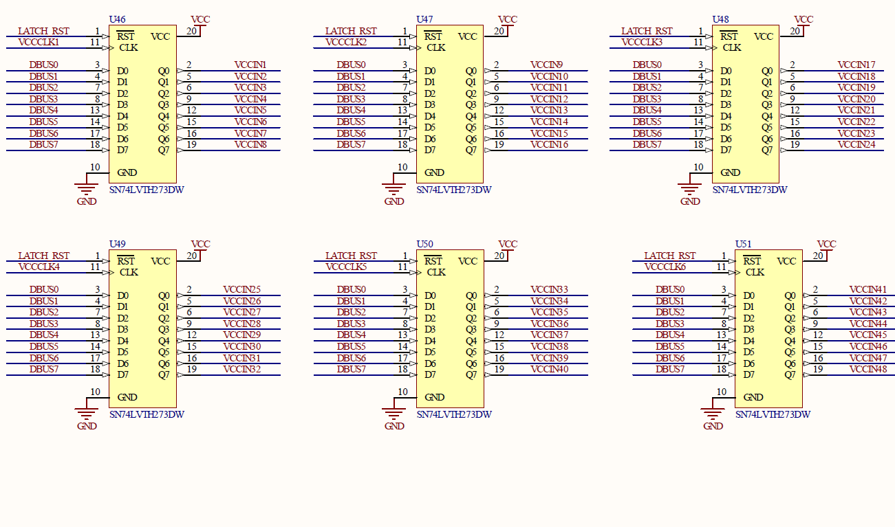
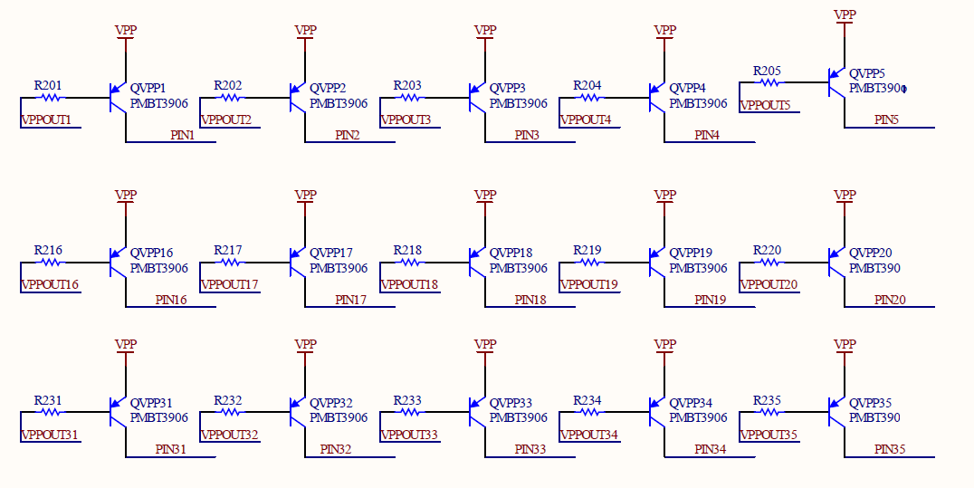
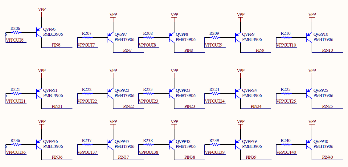
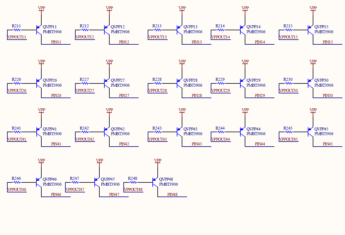
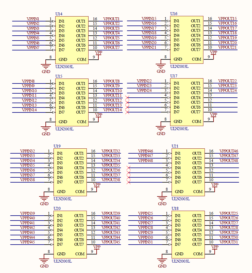
BeeHive204 ISP connector
As ISP connector is used 20 pins connector 2-1634689-0 from TE connectivity or other compatible connector.
ISP connector
Open Source Universal 48 pin programmer design的更多相关文章
- BeeProg2C Extremely fast universal USB interfaced programmer
http://www.elnec.com/products/universal-programmers/beeprog2c/ FPGA based totally reconfigurable 48 ...
- SmartProg2 Universal, ISP capable programmer
http://www.elnec.com/products/universal-programmers/smartprog2/ 40 powerful TTL pindrivers provide H ...
- Vivado Design Suite用户指南之约束的使用第二部分(约束方法论)
Constraints Methodology(约束方法论) 关于约束方法论 设计约束定义了编译流程必须满足的要求,以使设计在板上起作用. 并非所有步骤都使用所有约束在编译流程中. 例如,物理约束仅在 ...
- Design Patterns Example Code (in C++)
Overview Design patterns are ways to reuse design solutions that other software developers have crea ...
- (转) [it-ebooks]电子书列表
[it-ebooks]电子书列表 [2014]: Learning Objective-C by Developing iPhone Games || Leverage Xcode and Obj ...
- .net Framework Class Library(FCL)
from:http://msdn.microsoft.com/en-us/library/ms229335.aspx 我们平时在VS.net里引用的那些类库就是从这里来的 The .NET Frame ...
- SAE J1850 VPW Implement
---恢复内容开始--- OBDII Interface Project When I can ever find enough time away from schoolwork, I try to ...
- FT232H USB转串口,I2C,JTAG高速芯片
随着FT232H USB2.0高速芯片的发布,英商飞特蒂亚公司(FTDI)进一步巩固了其在USB接口集成电路产品的地位.此款多功能的单通道USB转UART/FIFO接口设备可通过EEPROM配置为各种 ...
- 6.Type and Member Basics
1.The Different Kinds of Type Members 1.Constants:a symbol that identifies a never-changing data val ...
随机推荐
- css预处理scss环境配置
css 预处理器 CSS 预处理器用一种专门的编程语言,进行 Web css编码,然后再编译成正常的 CSS 文件,以供项目使用:说简单点就是在某个环境下写css 可以写变量.表达式.嵌套等,在通过该 ...
- spring-mybatis.xml配置
1.自动扫描 <context:component-scan base-package="com.javen" /> 2.引入配置文件 <bean id=&quo ...
- /proc/sys 子目录的作用
该子目录的作用是报告各种不同的内核参数,并让您能交互地更改其中的某些.与 /proc 中所有其他文件不同,该目录中的某些文件可以写入,不过这仅针对 root. 其中的目录以及文件的详细列表将占据过多的 ...
- geoip 扩展包根据ip定位详情
教程:https://laravel-china.org/courses/laravel-package/2024/get-the-corresponding-geo-location-informa ...
- javaScript如何跳出多重循环break、continue
先来说说break和continue之间的区别 for(var i=0;i<10;i++){ if(i>5){ break; }}console.log(i); ---6 •当i ...
- java网络编程三次握手四次挥手
第一次握手:client设置syn=1,随机产生一个序列号seq=x,将数据包发送到server.client进入syn_send状态, 等待server确认. 第二次握手:server查看clien ...
- 日志生成控制文件syslog.conf
1: syslog.conf的介绍 对于不同类型的Unix,标准UnixLog系统的设置,实际上除了一些关键词的不同,系统的syslog.conf格式是相同的.syslog采用可配置的.统一的系统登记 ...
- 分布式跟踪系统zipkin+mysql
1.初始化数据库: 1) CREATE TABLE IF NOT EXISTS zipkin_spans ( trace_id_high BIGINT NOT NULL DEFAULT 0 COMME ...
- Pandas DataFrame构造简析
参考书籍:<利用Python进行数据分析> DataFrame简介: DataFrame是一个表格型的数据结构,它含有一组有序的列,每列可以是不同的值类型(数值.字符串.布尔值等).Dat ...
- day3 作业
文件操作用户很广泛,我们经常对文件进行操作: global log 127.0.0.1 local2 daemon maxconn log 127.0.0.1 local2 info defaults ...
