SWD Connect/Transfer Source Code
Serial Wire Debug interface
The Serial Wire Debug protocol operates with a synchronous serial interface.
This uses a single bidirectional data signal, and a clock signal.
This section gives an overview of the physical Serial Wire Debug interface.
Line interface
The Serial Wire Debug interface uses a single bidirectional data pin, SWDIO.
That is, the same signal is used for both host and target sourced signals.
The Serial Wire Debug interface is synchronous, and requires a clock pin, SWCLK.
The clock can be sourced from the target and exported, or provided by the host.
This clock is then used by the host as a reference for generation and sampling of data
so that the target is not required to perform any over-sampling.
Both the target and host are capable of driving the bus HIGH and LOW or tristating it.
The ports must be able to tolerate short periods of contention that might occur because of a loss of synchronization.
The clock can be asynchronous to any system clock, including the debug logic clock.
The Serial Wire Debug interface clock can be stopped when the debug port is idle,
see Introduction to the ARM Serial Wire Debug (SWD) protocol on page 4-89.
Line pull-up
So that the line is in a known state when neither host nor target is driving the line,
a 100KΩ pull-up is required at the target, but this can only be relied on to maintain the state of the wire.
If the wire is driven LOW and released, the pull-up resistor eventually returns the line to the HIGH state,
but this takes many clock periods.
The pull-up is intended to prevent false detection of signals when no host is connected.
This means it must be of a suitably high value to reduce current consumption
from the target when the host actively pulls down the line.
Note
A small current drains from the target whenever the line is driven LOW.
If the interface is left connected for extended periods when the target has to use a low-power mode,
the line must be held HIGH, or reset, by the host until the interface is activated.
Serial Wire Debug (SWD) protocol
The ARM Serial Wire Debug interface uses a single bidirectional data connection and a separate clock to transfer data synchronously.
An operation on the wire consists of two or three phases:
Packet request : The external host debugger issues a request to the DP. The DP is the target of the request.
Acknowledge response : The target sends an acknowledge response to the host.
Data transfer phase : This phase is only present when either:
- A data read or data write request is followed by a valid (OK) acknowledge response.
- The CTRL/STAT.ORUNDETECT flag is set to 1.
The data transfer is one of:
- Target to host, following a read request (RDATA).
- Host to target, following a write request (WDATA).
Note
If the CTRL/STAT.ORUNDETECT bit is set to 1, then a data transfer phase is required on all responses,
including WAIT and FAULT. For more information, see Sticky overrun behavior on page 4-98.
When the SW-DP receives a packet request from the debug host, it must respond immediately with the acknowledge phase.
There is a turnaround period between these phases, as they are in different directions.
If a data phase is required, this follows immediately after the acknowledge phase.
For a write request, there is a turnaround period between the acknowledge phase and the WDATA data transfer phase.
Following the WDATA data transfer phase the host continues to drive the wire.
There is no additional turnaround period.
For a read request, there is no turnaround period between the acknowledge phase and the data transfer phase.
There is a turnaround period following the RDATA data transfer phase, following which the host drives the wire.
To ensure that the transfer can be clocked through the SW-DP, after the data transfer phase the host must do one of the following:
- Immediately start a new SWD operation with the start bit of a new packet request.
- Continue to drive the SWD interface with idle cycles until the host starts a new SWD operation.
- If the host is driving the Serial Wire Debug clock, continue to clock the SWD interface
with at least eight idle cycles. After this it can stop the clock.
Line turn-round
To prevent contention, a turnaround period is required when the device driving the wire changes.
For the turnaround period, neither the host nor the target drives the wire, and the state of the wire is undefined.
See also Line pull-up on page 4-104.
Note
The line turn-round period can provide for pad delays when using a high sample clock frequency.
The length of the turnaround period is controlled by DLCR.TURNROUND : 1..4
The default setting is a turnaround period of one clock cycle.
DLCR, Data Link Control Register
The DLCR attributes are: Purpose Controls the operating mode of the Data Link.
Configurations A DP architecture register. The DLCR is defined and implemented only in DPv1 and DPv2.
Attributes The DLCR is:
• DATA LINK DEFINED.
• A read/write register.
• Accessed by a read or write to offset 0x4 of the DP address map when SELECT.DPBANKSEL is set to 0x1.
See the field descriptions for information about the register reset value.
For SW-DP, the DLCR bit assignments are:

Idle cycles
After completing a transaction, the host must either insert at least 8 idle cycles
or continue immediately with the start bit of a new transaction.
The host clocks the Serial Wire Debug interface with the line LOW to insert idle cycles.
A transaction must be followed by another transaction or at least 8 idle cycles
to ensure that data is clocked through the AP.
Bit order
All data values in SWD operations are transferred LSB first.
For example, the OK response of 0b001 appears on the wire as 1, followed by 0, followed by 0,
as shown in Figure 4-1 on page 4-94 and Figure 4-2 on page 4-95.
Parity
A simple parity check is applied to all packet request and data transfer phases.
Even parity is used:
Packet requests
The parity check is made over the APnDP, RnW and A[2:3] bits. If, of these four bits:
• The number of bits set to 1 is odd, then the parity bit is set to 1.
• The number of bits set to 1 is even, then the parity bit is set to 0.
Data transfers (WDATA and RDATA)
The parity check is made over the 32 data bits, WDATA[0:31] or RDATA[0:31]. If, of these 32 bits:
• The number of bits set to 1 is odd, then the parity bit is set to 1.
• The number of bits set to 1 is even, then the parity bit is set to 0.
The packet request parity bit is shown in each of the diagrams in this section,
from Figure 4-1 on page 4-94 to Figure 4-7 on page 4-99.
It appears on the wire immediately after the A[2:3] bits.
A parity error in the packet request is detected by the SW-DP, which responds with a protocol error.
See Protocol error response on page 4-97.
The WDATA parity bit is shown in Figure 4-1 on page 4-94 and in Figure 4-7 on page 4-99.
It appears on the wire immediately after the WDATA[31] bit.
A parity error in the WDATA data transfer phase is detected by the SW-DP and,
other than writes to TARGETSEL, recorded in CTRL/STAT.WDATAERR.
If overrun detection is enabled, CTRL/STAT.STICKYORUN is set to 1.
A parity error in a write to TARGETSEL deselects the target.
The RDATA parity bit is shown in Figure 4-2 on page 4-95.
It appears on the wire immediately after the RDATA[31] bit.
The debugger must check for parity errors in the RDATA data transfer phase and retry the read if required.
Note
The ACK[0:2] bits are never included in the parity calculation.
Debuggers must remember this when parity checking the data from a read operation,
when the debugger receives a continuous stream of 36 bits, as shown in Figure 4-2 on page 4-95:
• Bits 0 to 2 are ACK[0:2].
• Bits 3 to 34 are RDATA[0:31].
• Bit 35 is the parity bit.
The parity check must be applied to bits 3 to 34 of this block of data, and the result compared with bit 35, the parity bit.

Limitations of multi-drop
This section describes the configuration and auto-detection limitations of a multi-drop Serial Wire Debug system.
System configuration
Each device must be configured with a unique target ID, that includes a 4-bit instance ID,
to differentiate between otherwise identical targets.
This places a limit of 16 such targets in any system, and means that identical devices must be configured
before they are connected together to ensure that their instance IDs do not conflict.
Auto-detection of the target
It is not possible to interrogate a multi-drop Serial Wire Debug system
that includes multiple devices to establish which devices are connected.
Because all devices are selected on coming out of a line reset,
no communication with a device is possible without prior selection of that target using its target ID.
Therefore, connection to a multi-drop Serial Wire Debug system that includes multiple devices requires that either:
• The host has prior knowledge of the devices in the system and is configured before target connection.
• The host attempts auto-detection by issuing a target select command for each of the devices it has been configured to support.
While this is likely to involve a large number of target select commands, it must be possible to iterate
through all the supported devices in a reasonable time from the viewpoint of a user of the debug tools.
Note
This means that debug tools cannot connect seamlessly to targets in a multi-drop Serial Wire Debug system
that they have never seen before.
However, if the debug tools can be provided with the target ID of such targets by the user
then the contents of the target can be auto-detected as normal.
To protect against multiple selected devices all driving the line simultaneously SWD protocol version 2 requires:
• For multi-drop SWJ-DP, the JTAG connection is selected out of powerup reset. JTAG does not drive the line.
See Chapter 5 The Serial Wire/JTAG Debug Port (SWJ-DP).
• For multi-drop SW-DP, the DP is in the dormant state out of powerup reset. See Dormant operation on page 5-113.
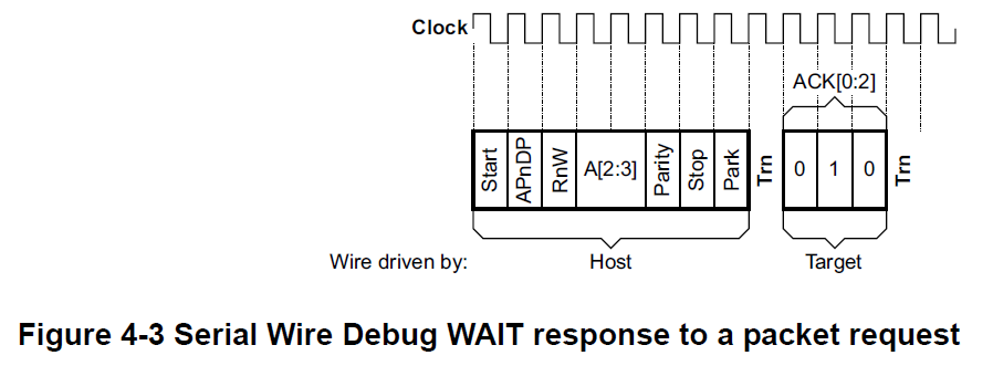
WAIT response to read or write operation request
If the SW-DP is not able to process the request from the debugger immediately it must issue a WAIT response.
A WAIT response to a read or write packet request consists of two phases:
1. An eight-bit read or write packet request, from the host to the target.
2. A three-bit WAIT acknowledge response, from the target to the host.
By default, there are single-cycle turnaround periods between these two phases, and after the second phase.
See Line turn-round on page 4-90 for more information.
A WAIT response to a read or write packet request is shown in Figure 4-3.
If overrun detection is enabled then CTRL/STAT.STICKYORUN is set to 1
and a data phase is required on a WAIT response.
For more information see Sticky overrun behavior on page 4-98.
A WAIT response must not be issued to the following requests.
The SW-DP must always process these requests immediately:
• Reads of the DPIDR register.
• Reads of the CTRL/STAT register.
• Writes to the ABORT register. --- enables the debugger to access other parts of the debug system.
With any other request, the DP issues a WAIT response if it cannot process the request. This happens if:
• A previous AP or DP access is outstanding.
• The new request is an AP read request and the result of the previous AP read is not yet available.
Normally, when a debugger receives a WAIT response it retries the same operation.
This enables it to process data as quickly as possible.
However, if several retries have been attempted, with a wait that is long enough for a slow interconnection
and memory system to respond, if appropriate, the debugger might write to ABORT.DAPABORT.
This signals to the active AP that it must terminate the transfer that it is currently attempting.
An AP implementation might be unable to terminate a transfer on its SoC interface.
However, on receiving a DAP abort request the AP must free up the interface to the Debug Port.
Writing to the ABORT register after receiving a WAIT response
enables the debugger to access other parts of the debug system.
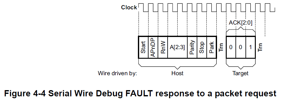
FAULT response to read or write operation request
A SW-DP must not issue a FAULT response for:
• Reads of the DPIDR register, which is a read-only register.
• Reads of the CTRL/STAT register, which is a read/write register.
• Writes to the ABORT register, which is a write-only register.
For any other access, the SW-DP issues a FAULT response
if any sticky flag is set to 1 in the CTRL/STAT register.
A FAULT response to a read or write packet request consists of two phases:
1. An eight-bit read or write packet request, from the host to the target.
2. A three-bit FAULT acknowledge response, from the target to the host.
By default, there are single-cycle turnaround periods between these two phases, and after the second phase.
See Line turn-round on page 4-90 for more information.
A FAULT response to a read or write packet request is shown in Figure 4-4.
If overrun detection is enabled then CTRL/STAT.STICKYORUN is set to 1
and a data phase is required on a FAULT response.
For more information see Sticky overrun behavior on page 4-98.
Use of the FAULT response enables the protocol to remain synchronized.
A debugger might stream a block of data and then check the CTRL/STAT register at the end of the block.
In a SW-DP, the sticky error flags are cleared to 0 by writing bits in the ABORT register.
Protocol error response
A protocol error occurs if any of the following occurs:
• The Parity bit does not match the parity of the packet request.
• The Stop bit is not 0.
• The Park bit is not 1.
• DLCR.TURNROUND indicates an unsupported turnaround period.
Note
If the Parity bit in the WDATA transfer phase does not match the parity of the data,
this does not cause a protocol error response, as the SW-DP has already given its response to the header.
For more information, see Sticky flags and DP error responses on page 2-34.
If overrun detection is enabled then CTRL/STAT.STICKYORUN is set to 1
and the target must wait until the data phase of the transaction has completed
before entering the protocol error state.
Otherwise, it enters the protocol errorstate immediately.
When a protocol error is detected by the SW-DP, the SW-DP does not reply to the packet request
and does not drive the line. This is illustrated in Figure 4-5 on page 4-98.
Note
If SWD protocol version 2 is implemented, the SW-DP also does not reply to a TARGETSEL register write packet request.

When in protocol error state:
• If the target detects a valid read of the DP DPIDR register, it is IMPLEMENTATION DEFINED
whether the target leaves the protocol error state, and gives an OK response.
• If the target detects a valid packet header, other than the read of the DP DPIDR register,
or the target detects an IMPLEMENTATION DEFINED number of additional protocol errors, it enters the lockout state.
ARM recommends that the target enters the lockout state after one more protocol error is detected while in the protocol error state.
If the target cannot leave the protocol error state on a read of the DPIDR register, then the protocol error and lockout states are equivalent.
The target must leave the protocol error state on an line reset.
The target only leaves the lockout state on a line reset.
If the SW-DP implements SWD protocol version 2, it must enter the lockout state after a single protocol error immediately after a line reset.
However, if the first packet request detected by the target following line reset is valid
it can then revert to entering the lockout state after an IMPLEMENTATION DEFINED number of protocol errors.
Host response to protocol error
If the host does not receive an expected response from the target,
it must leave the line not driven for at least the length of any potential data phase
and then attempt a line reset.
For more information, see Connection and line resetsequence on page 4-104.
The host can attempt reads of the DP DPIDR register before attempting a line reset,
as the target might respond and leave the protocol error state, but ARM does not recommend this.
If the transfer that resulted in the original protocol error response was a write you can assume that no write occurred.
If the original transfer was a read it is possible that the read was issued to an AP. Although this is unlikely,
you must consider this possibility because reads are pipelined.
Sticky overrun behavior
If a SW-DP receives a transaction request when the previous transaction has not completed it returns a WAIT response.
If overrun detection is enabled in the CTRL/STAT register, the CTRL/STAT.STICKYORUN flag is set to 1.
ORUNDETECT, bit[0]
This bit is set to 1 to enable overrun detection. For more information see Overrun detection on page 2-34.
After a powerup reset, this bit is set to 0.
Subsequent transactions generate FAULT responses, because a sticky flag is set to 1.
If overrun detection is enabled, CTRL/STAT.STICKYORUN is also set
if there is a FAULT response, protocol error, or line reset.
When overrun detection is enabled, WAIT and FAULT responses require a data phase:
• If the transaction is a read the data in the data phase is UNKNOWN.
The target does not drive the line, and the host must not check the parity bit.
• If the transaction is a write the data phase is ignored.
Figure 4-6 on page 4-99 shows the WAIT or FAULT response to a read operation when overrun detection is enabled,
and Figure 4-7 on page 4-99 shows the response to a write operation when overrun detection is enabled.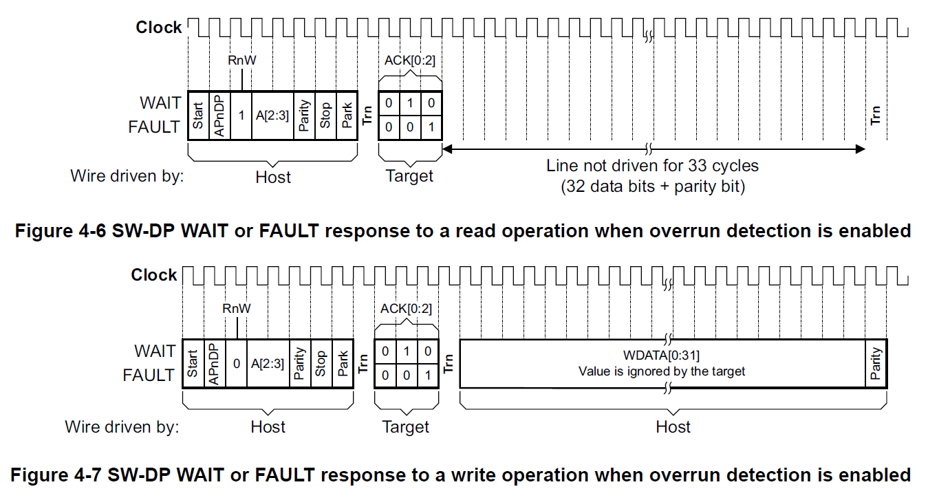
/* OK response ****************************************************************/
// data_phase : read : Read RDATA[0:31] + Parity, Turnaround, Idle cycles
// data_phase : write : Turnaround, Write WDATA[0:31] + Parity, Idle cycles
/* WAIT or FAULT response *****************************************************/
If overrun detection is enabled
// data_phase : read : Dummy Read RDATA[0:31] + Parity, Turnaround
// data_phase : write : Turnaround, Dummy Write WDATA[0:31] + Parity
/* Protocol error *************************************************************/
If overrun detection is enabled
// turnaround, DATA, Parity
Line not driven by target, if SWD pull up is used, Host get 111, else, != 100, 010, 001 : 011, 101, 110, 000
CTRL/STAT, Control/Status register
The CTRL/STAT register attributes are:
Purpose The Control/Status register provides control of the DP and status information about the DP.
Configurations
A DP architecture register. The CTRL/STAT register is defined and implemented in DPv0, DPv1,and DPv2.
Attributes The CTRL/STAT register is:
• A read/write register, in which some fields are RO, meaning they ignore writes. See the field descriptions for more information.
• Accessed by a read or write to offset 0x4 of the DP register map, when SELECT.DPBANKSEL is 0x0.

ORUNDETECT, bit[0]
This bit is set to 1 to enable overrun detection. For more information see Overrun detection on page 2-34.
After a powerup reset, this bit is set to 0.
Overrun detection
Debug Ports support an overrun detection mode.
This mode enables a user to send blocks of commands to an emulator
on a high latency, high throughput, connection.
These commands must be sent with sufficient in-line delays to make overrun errors unlikely.
However, the DAP can be programmed so that, if an overrun error occurs,
the DAP flags the error by setting the Sticky Overrun flag, CTRL/STAT.STICKYORUN to 1.
In this overrun detection mode the debugger must check for overrun errors
after each sequence of APACC transactions, by checking this flag.
Overrun detection mode is enabled by setting the Overrun Detect bit, CTRL/STAT.ORUNDETECT, to 1.
The Sticky Overrun flag, CTRL/STAT.STICKYORUN is set to 1 if the response to any transaction is other than OK.
The first response to a transaction when a previous AP transaction has not completed is WAIT.
Following responses are FAULT, because the STICKYORUN bit is set to 1.
WAIT --> FAULT
STICKYORUN, bit[1]
If overrun detection is enabled, this bit is set to 1 when an overrun occurs.
The behavior on writing is DATA LINK DEFINED:
• On a JTAG-DP, access is R/W1C.
• On an SW-DP, access is RO/WI.
The clearing of this bit to 0 is DATA LINK DEFINED,
see Clearing the sticky error and compare flags in the CTRL/STAT register on page 2-50.
After a powerup reset, this bit is set to 0.
ABORT, AP Abort register

ORUNERRCLR, bit[4], DPv1 or higher
Write 1 to this bit to clear the CTRL/STAT.STICKYORUN overrun error bit to 0.
STKERRCLR, bit[2], DPv1 or higher
Write 1 to this bit to clear the CTRL/STAT.STICKYERR sticky error bit to 0.
Clearing the sticky error and compare flags in the CTRL/STAT register
The descriptions of these bits in CTRL/STAT indicate the condition that sets each bit to 1.
When one of these bits is set to 1, a write of 0 to that bit is ignored.
These bits can be cleared to 0 as follows:
Write 1 to the appropriate CLR field of the ABORT register:
• To clear STICKYERR to 0, write 1 to the ABORT.STKERRCLR field.
• To clear STICKYCMP to 0, write 1 to the ABORT.STKCMPCLR field.
• To clear STICKYORUN to 0, write 1 to the ABORT.ORUNERRCLR field.
• To clear WDATAERR to 0, write 1 to the ABORT.WDERRCLR field, SW-DP only.
You can use a single write of the ABORT register to clear multiple flags to 0 if necessary.
After clearing the flag to 0, you might have to access the DP and AP registers to find what caused the flag to be set to 1.
Typically:
• For the STICKYERR or STICKYCMP flag, you must find which location was accessed to cause the flag to be set to 1.
• For the STICKYORUN flag, you must find which DP or AP transaction caused the overrun.
You then have to repeat your transactions from that point.
• For the WDATAERR flag, you must resend the corrupted data.
//-----------------------------------------------------------------------------

//

// Sets the target device for Serial Wire communication and returns the

// 32-bit ID code. Must be called before performing any SWD commands.

//

// Returns:

//  1-4. IDCODE - Value read from the IDCODE register (32-bit).

//    5. Response code.

//

STATUS SWD_Connect(void)

{

    U8 rtn;

    // Initialize IO pins for SWD interface

    _SetSWPinsIdle;

    // Select the Serial Wire Debug Port

    // Skip this switch sequence if the device does not have the swj_dp port

    // Serial Wire + JTAG

    SW_ShiftReset();

    SW_ShiftByteOut(0x9E);

    SW_ShiftByteOut(0xE7);

    // Reset the line and return the 32-bit ID code

    rtn = SWD_LineReset();

    //SendLongToHost(io_word.U32);

    return rtn;

}
// Switches the debug interface to JTAG communication and disconnects pins.

//

// Returns:

//    1. HOST_COMMAND_OK

//

STATUS SWD_Disconnect(void)

{

    // Initialize IO pins for SWD interface

    _SetSWPinsIdle;

    // Select the JTAG Debug Port

    // Skip this switch sequence if the device does not have the swj_dp port

    // Serial Wire + JTAG

    SW_ShiftReset();

    SW_ShiftByteOut(0x3C);

    SW_ShiftByteOut(0xE7);

    // Release debug interface pins except nSRST

    _ResetDebugPins;

    return HOST_COMMAND_OK;

}
//-----------------------------------------------------------------------------

//

// Performs a line reset on the Serial Wire interface.

//

// Returns:

//    1. Response code.

//

STATUS SWD_LineReset(void)

{

    U8 ack;

    // Complete SWD reset sequence (50 cycles high followed by 2 or more idle cycles)

    SW_ShiftReset();

    SW_ShiftByteOut();

    // Now read the DPIDR register to move the SWD out of reset

    ack = SW_ShiftPacket(SW_IDCODE_RD, );

    SW_ShiftByteOut();

    return SW_Response(ack);

}
#define SW_CLOCK_CYCLE()                \

  PIN_SWCLK_CLR();                      \

  PIN_DELAY();                          \

  PIN_SWCLK_SET();                      \

  PIN_DELAY()

#define SW_WRITE_BIT(bit)               \

  PIN_SWDIO_OUT(bit);                   \

  PIN_SWCLK_CLR();                      \

  PIN_DELAY();                          \

  PIN_SWCLK_SET();                      \

  PIN_DELAY()

#define SW_READ_BIT(bit)                \

  PIN_SWCLK_CLR();                      \

  PIN_DELAY();                          \

  bit = PIN_SWDIO_IN();                 \

  PIN_SWCLK_SET();                      \

  PIN_DELAY()

/* OK response ****************************************************************/

// data_phase : read : Read RDATA[0:31] + Parity, Turnaround, Idle cycles

// data_phase : write : Turnaround, Write WDATA[0:31] + Parity, Idle cycles

/* WAIT or FAULT response *****************************************************/

// data_phase : read : Dummy Read RDATA[0:31] + Parity, Turnaround

// data_phase : write : Turnaround, Dummy Write WDATA[0:31] + Parity

/* Protocol error *************************************************************/

// turnaround, DATA, Parity

uint8_t SWD_Transfer( uint32_t request, uint32_t *data )

{

  uint32_t ack;

  uint32_t bit;

  uint32_t val;

  uint32_t parity;

  uint32_t n;

  /* Packet Request */

  parity = ;

  SW_WRITE_BIT(  ); /* Start Bit */

  bit = request >> ;

  SW_WRITE_BIT( bit ); /* APnDP Bit */

  parity += bit;

  bit = request >> ;

  SW_WRITE_BIT( bit ); /* RnW Bit */

  parity += bit;

  bit = request >> ;

  SW_WRITE_BIT( bit ); /* A2 Bit */

  parity += bit;

  bit = request >> ;

  SW_WRITE_BIT( bit ); /* A3 Bit */

  parity += bit;

  SW_WRITE_BIT( parity ); /* Parity Bit */

  SW_WRITE_BIT(  ); /* Stop Bit */

  SW_WRITE_BIT(  ); /* Park Bit */

  /* Turnaround : 1..4 Cycles                                                                        */

  PIN_SWDIO_OUT_DISABLE( );

  for ( n = DAP_Data.swd_conf.turnaround; n; n-- )

  {

    SW_CLOCK_CYCLE( )

    ;

  }

  /* Acknowledge response */

  SW_READ_BIT( bit );

  ack = bit << ;

  SW_READ_BIT( bit );

  ack |= bit << ;

  SW_READ_BIT( bit );

  ack |= bit << ;

  if ( ack == DAP_TRANSFER_OK ) /* OK response ********************************/

  {

    /* Data transfer */

    if ( request & DAP_TRANSFER_RnW ) /* Read data ****************************/

    {

      val = ;

      parity = ;

      for ( n = ; n; n-- ) /* Read RDATA[0:31] */

      {

        SW_READ_BIT( bit );

        parity += bit;

        val >>= ;

        val |= bit << ;

      }

      SW_READ_BIT( bit ); /* Read Parity */

      if ( ( parity ^ bit ) &  )

      {

        ack = DAP_TRANSFER_ERROR;

      }

      if ( data )

        *data = val;

      for ( n = DAP_Data.swd_conf.turnaround; n; n-- ) /* Turnaround */

      {

        SW_CLOCK_CYCLE( )

        ;

      }

      PIN_SWDIO_OUT_ENABLE( );

    }

    else /* Write data ********************************************************/

    {

      for ( n = DAP_Data.swd_conf.turnaround; n; n-- ) /* Turnaround */

      {

        SW_CLOCK_CYCLE( )

        ;

      }

      PIN_SWDIO_OUT_ENABLE( );

      val = *data;

      parity = ;

      for ( n = ; n; n-- ) /* Write WDATA[0:31] */

      {

        SW_WRITE_BIT( val );

        parity += val;

        val >>= ;

      }

      SW_WRITE_BIT( parity ); /* Write Parity Bit */

    } // if ( request & DAP_TRANSFER_RnW ) /* Read data */ else /* Write data */

    /* Idle cycles : n >= 8                                                                               */

    n = DAP_Data.transfer.idle_cycles;

    if ( n )

    {

      PIN_SWDIO_OUT(  );

      for ( ; n; n-- )

      {

        SW_CLOCK_CYCLE( )

        ;

      }

    }

    PIN_SWDIO_OUT(  );

    return ( ack );

  } // if ( ack == DAP_TRANSFER_OK ) /* OK response ***************************/

  /* WAIT or FAULT response ***************************************************/

  // data_phase : read : Dummy Read RDATA[0:31] + Parity, Turnaround

  // data_phase : write : Turnaround, Dummy Write WDATA[0:31] + Parity

  if ( ( ack == DAP_TRANSFER_WAIT ) || ( ack == DAP_TRANSFER_FAULT ) )

  {

    if ( DAP_Data.swd_conf.data_phase

      && ( ( request & DAP_TRANSFER_RnW ) !=  ) )

    {

      for ( n =  + ; n; n-- ) /* Dummy Read RDATA[0:31] + Parity */

      {

        SW_CLOCK_CYCLE( )

        ;

      }

    }

    /* Turnaround */

    for ( n = DAP_Data.swd_conf.turnaround; n; n-- )

    {

      SW_CLOCK_CYCLE( )

      ;

    }

    PIN_SWDIO_OUT_ENABLE( );

    if ( DAP_Data.swd_conf.data_phase

      && ( ( request & DAP_TRANSFER_RnW ) ==  ) )

    {

      PIN_SWDIO_OUT(  );

      for ( n =  + ; n; n-- ) /* Dummy Write WDATA[0:31] + Parity */

      {

        SW_CLOCK_CYCLE( )

        ;

      }

    }

    PIN_SWDIO_OUT(  );

    return ( ack );

  }

  /* Protocol error : turnaround, DATA, Parity ********************************/

  //

  for ( n = DAP_Data.swd_conf.turnaround +  + ; n; n-- )

  {

    SW_CLOCK_CYCLE( )

    ; /* Back off data phase */

  }

  PIN_SWDIO_OUT(  );

  return ( ack );

}
SWD Connect/Transfer Source Code的更多相关文章
- attack source code
不废话,直接上代码, 先看截图use pictures;
- How to Build MySQL from Source Code on Windows & compile MySQL on win7+vs2010
Not counting obtaining the source code, and once you have the prerequisites satisfied, [Windows] use ...
- Website's Game source code
A Darkroom by doublespeakgames <!DOCTYPE html> <html itemscope itemtype="https://schem ...
- android activity 启动过程分析(source code 4.4)
说实话,android source code从2.3到4.4变化是蛮多的,尤其是media部分,虽然总的框架是没有多大变化,但是找起代码来看还是挺麻烦的.在android里面最受伤的是使用了java ...
- Tips for newbie to read source code
This post is first posted on my WeChat public account: GeekArtT Reading source code is always one bi ...
- 编程等宽字体Source Code Pro(转)
Source Code Pro - 最佳的免费编程字体之一!来自 Adobe 公司的开源等宽字体下载 每一位程序员都有一套自己喜爱的代码编辑器与编程字体,譬如我们之前就推荐过一款"神 ...
- How to build the Robotics Library from source code on Windows
The Robotics Library is an open source C++ library for robot kinematics, motion planning and control ...
- How to build windows azure PowerShell Source Code
Download any version source code of Windows Azure Powershell from https://github.com/Azure/azure-sdk ...
- akka cluster sharding source code 学习 (1/5) 替身模式
为了使一个项目支持集群,自己学习使用了 akka cluster 并在项目中实施了,从此,生活就变得有些痛苦.再配上 apache 做反向代理和负载均衡,debug 起来不要太酸爽.直到现在,我还对 ...
随机推荐
- hibernate的一对多和多对一关联
一对一的关联就不写了,一般项目也用不到,如果可以一对一就直接合成一个表了,也不会出现一对一的关系. 本文主要研究一对多的关系. 1.一对多的关系研究: (1)RDB中关系表达: 多的一方创建外键指向 ...
- mysql 获取当月日期天数
本月总共天数:SELECT TIMESTAMPDIFF(day,CURDATE(),(DATE_add(CURDATE(),INTERVAL 1 month)))
- 【前端开发】移动端适配方案js,rem单位转换,640设计稿20px=1rem
! function() { var style = document.createElement("STYLE"), docEl = document.documentEleme ...
- tensorflow 使用预训练好的模型的一部分参数
vars = tf.global_variables() net_var = [var for var in vars if 'bi-lstm_secondLayer' not in var.name ...
- java 轨迹栈
printStackTrace()方法所提供的信息可以通过getStackTrace()方法直接访问. getStackTrace()方法返回一个由根轨迹中的元素所构成的数组,每一个元素都表示栈中的一 ...
- [USACO17FEB]Why Did the Cow Cross the Road I G
一开始想写$DP$,发现直接转移完全有后效性 所以本小蒟蒻写了个最短路 每走三步就要吃草是这个题最难搞的地方,我们建图时不妨只对于距离等于三的点连边 考虑完全覆盖所有情况,从一个点走一步,两步,然后三 ...
- python强大的数据类型转换
# 原始的二维表数据集 jsonObj=[] # 添加模拟的数据 for i in range(1001,1004): for j in range(1,34): jsonObj.append({&q ...
- 解决 Delphi XE5 写Android程序的No resource identifier found for attribute... 错误【转】
原文:http://www.hxhlb.cn/article/32142aaeb67bbc05379369c3.html 那一天,我装上了RAD Studio XE5. 当天晚上,我就写了一个小小的A ...
- HDU 4348 To the moon(主席树区间修改)
题意 给你一个区间,支持如下操作: 在一段区间内加上一个值,并生成一个历史版本 查询某个版本下一段区间内的和 回到一个历史版本上并舍弃之后的版本 做法 这就是主席树区间修改裸题啦QwQ 上一篇博客我讲 ...
- 【Atcoder】ARC102 题解
C - Triangular Relationship 题解 枚举一个数%K的值然后统计另两个 代码 #include <bits/stdc++.h> #define enter putc ...