NVIDIA GPU Pascal架构简述
NVIDIA GPU Pascal架构简述
本文摘抄自英伟达Pascal架构官方白皮书:https://www.nvidia.com/en-us/data-center/resources/pascal-architecture-whitepaper/
SM
- 相比Maxwell架构,Pascal架构改进了16-nm FinFET的制造工艺,并提供了各种其它架构改进。
Pascal further improves the already excellent power efficiency provided by the Maxwell architecture through both an improved 16-nm FinFET manufacturing process and various architectural modifications.
- 与Maxwell架构类似,Pascal架构在每个分区中提供了2的次幂个CUDA核心,且每个线程束调度器都处理一个线程束数目(32)的CUDA核心中。
Like Maxwell, Pascal employs a power-of-two number of CUDA Cores per partition. This simplifies scheduling compared to Kepler, since each of the SM's warp schedulers issue to a dedicated set of CUDA Cores equal to the warp width (32).
- 每个线程束调度器支持双重处理(在内存加载/存储操作周期内CUDA核心处理数学操作),现在单次操作即可利用所有的CUDA核心。
Each warp scheduler still has the flexibility to dual-issue (such as issuing a math operation to a CUDA Core in the same cycle as a memory operation to a load/store unit), but single-issue is now sufficient to fully utilize all CUDA Cores.
- 每个GP104的SM提供了4个线程束调度器,用于管理总计128个fp32核心和4个fp64核心。而每个GP100的SM提供了2个线程束调度器,用于管理64个fp32核心和32个fp64核心。一个GP104提供了20个SM,相比之下GP102提供了30个SM,而GP100则提供了高达60个SM。
Like Maxwell, each GP104 SM provides four warp schedulers managing a total of 128 single-precision (FP32) and four double-precision (FP64) cores. A GP104 processor provides up to 20 SMs, and the similar GP102 design provides up to 30 SMs.By contrast GP100 provides smaller but more numerous SMs. Each GP100 provides up to 60 SMs. Each SM contains two warp schedulers managing a total of 64 FP32 and 32 FP64 cores.
- 与Maxwell架构相同,Pascal架构每SM支持最多64个线程束并行,
The maximum number of concurrent warps per SM remains the same as in Maxwell and Kepler (i.e., 64)
- Pascal架构每SM拥有64k个32-bit寄存器,每线程最多允许使用255个寄存器,每SM支持最多32个线程块驻留(相比Kepler架构,Pascal在线程块为64或更小情况下kernel的占有率提高),每SM的共享内存大小GP100为64KB,GP104为96KB,但每个线程块最多允许使用48KB共享内存。当然,英伟达推荐每个线程块最多使用32KB共享内存,因为这能使得每个SM至少可同时驻留2个线程块。
The register file size (64k 32-bit registers) is the same as that of Maxwell and Kepler GK110.
The maximum registers per thread, 255.
The maximum number of thread blocks per SM is 32. Compared to Kepler, Pascal should see an automatic occupancy improvement for kernels with thread blocks of 64 or fewer threads (shared memory and register file resource requirements permitting).
Shared memory capacity per SM is 64KB for GP100 and 96KB for GP104.The maximum shared memory per block remains limited at 48KB as with prior architectures. NVIDIA recommends that applications use at most 32 KB of shared memory in any one thread block.
- Pascal提升了对fp16浮点数格式(half)的支持。Pascal通过使用成对操作同时执行每个核心的两个fp16指令来达到fp16的吞吐量峰值,为符合成对操作的条件,操作数必须以half2格式存储。GP100提供了两倍fp32的fp16吞吐量支持,相比之下GP104仅提供了64分之1倍fp32的fp16支持,但GP104提供了额外的int8格式支持。
Pascal provides improved FP16 support for applications. Peak FP16 throughput is attained by using a paired operation to perform two FP16 instructions per core simultaneously.GP100, designed with training deep neural networks in mind, provides FP16 throughput up to 2x that of FP32 arithmetic. On GP104, FP16 throughput is lower, 1/64th that of FP32. However, compensating for reduced FP16 throughput, GP104 provides additional high-throughput INT8 support not available in GP100.
- GP104为int8提供了专用的2路和4路整数点乘指令,__dp4a指令点乘4个8-bit整数并累加到一个32-bit整数中,类似的,__dp2a指令点乘2个16-bit整数和2个8-bit整数并累加到一个32-bit整数中。
GP104 provides specialized instructions for two-way and four-way integer dot products.The __dp4a intrinsic computes a dot product of four 8-bit integers with accumulation into a 32-bit integer. Similarly, __dp2a performs a two-element dot product between two 16-bit integers in one vector, and two 8-bit integers in another with accumulation into a 32-bit integer.
- GP100为DRAM提供了High Bandwidth Memory 2 (HBM2)存储器,HBM2存储芯片与GPU芯片封装在同一硅片上,与传统GDDR技术相比,这能提供更高的带宽。GP100最多连接到4个HBM2堆栈,每个堆栈使用两个512-bit存储控制器。存储总线的有效宽度为4096位,相比GM200的384-bit,这可以极大的提高带宽峰值。因此,使用GP100架构的Tesla P100拥有高达732GB/s的带宽峰值和 715 MHz的内存周期。
GP100 uses High Bandwidth Memory 2 (HBM2) for its DRAM. HBM2 memories are stacked on a single silicon package along with the GPU die. This allows much wider interfaces at similar power compared to traditional GDDR technology. GP100 is linked to up to four stacks of HBM2 and uses two 512-bit memory controllers for each stack.The effective width of the memory bus is then 4096 bits, a significant increase over the 384 bits in GM200. This allows a tremendous boost in peak bandwidth even at reduced memory clocks. Thus, the GP100 equipped Tesla P100 has a peak bandwidth of 732 GB/s with a modest 715 MHz memory clock.
- GP100提供了ECC校验,通常情况下这会造成6.25%的内存消耗和20%的带宽损失,而HBM2 提供了专用的ECC资源,因此可以实现无开销的ECC校验。
Like Kepler GK210, the GP100 GPU's register files, shared memories, L1 and L2 caches, and DRAM are all protected by Single-Error Correct Double-Error Detect (SECDED) ECC code. When enabling ECC support on a Kepler GK210, the available DRAM would be reduced by 6.25% to allow for the storage of ECC bits. Fetching ECC bits for each memory transaction also reduced the effective bandwidth by approximately 20% compared to the same GPU with ECC disabled. HBM2 memories, on the other hand, provide dedicated ECC resources, allowing overhead-free ECC protection.4
- 默认情况下,GP100将全局内存加载到L1/纹理缓存,与此相反,GP104仅仅加载到L2缓存(同Kepler和Maxwell架构),但GP104允许用户在nvcc编译时使用-Xptxas -dlcm=ca选项开启L1/纹理缓存。
By default, GP100 caches global loads in the L1/Texture cache. In contrast, GP104 follows Kepler and Maxwell in caching global loads in L2 only, unless using the LDG read-only data cache mechanism introduced in Kepler. As with previous architectures, GP104 allows the developer to opt-in to caching all global loads in the unified L1/Texture cache by passing the -Xptxas -dlcm=ca flag to nvcc at compile time.
- 当启用L1缓存时,Kepler通过128B粒度的内存服务来加载全局数据,否则内存服务粒度为32B。但在Pascal架构中,内存服务的粒度始终为32B。
Kepler serviced loads at a granularity of 128B when L1 caching of global loads was enabled and 32B otherwise. On Pascal the data access unit is 32B regardless of whether global loads are cached in L1.
- 同Maxwell架构,Pascal提供了原生的 32-bit整数共享内存原子指令,和32-bit、64-bit的CAS指令。Pascal还提供了FP64全局内存原子指令,现atomicAdd()函数支持32-bit和64-bit的整数和浮点数操作。
Like Maxwell, Pascal provides native shared memory atomic operations for 32-bit integer arithmetic, along with native 32 or 64-bit compare-and-swap (CAS). Pascal also extends atomic addition in global memory to function on FP64 data. The atomicAdd() function in CUDA has thus been generalized to support 32 and 64-bit integer and floating-point types.
- 对于GP100,原子指令可以针对通过nvlink连接的存储器上的数据实现原子操作,但PCIe连接不支持。通常,跨存储器的原子操作通过一个page-faults来将另一存储器上的数据移动到本地实现。
For GP100 atomic operations may target the memories of peer GPUs connected through NVLink. Peer-to-peer atomics over NVLink use the same API as atomics targeting global memory. GPUs connected via PCIE do not support this feature.When an atomic targets a migratable address backed by a remote memory space, the local processor page-faults so that the kernel can migrate the appropriate memory page to local memory.
- 不同于Kepler架构L1和共享内存使用同一块片上存储,Maxwell和Pascal架构由于L1和纹理缓存合并,因此为每个SM提供了专用的共享内存存储,GP100现每SM拥有64KB共享内存,GP104每SM拥有96KB共享内存。
For Kepler, shared memory and the L1 cache shared the same on-chip storage. Maxwell and Pascal, by contrast, provide dedicated space to the shared memory of each SM, since the functionality of the L1 and texture caches have been merged. This increases the shared memory space available per SM as compared to Kepler: GP100 offers 64 KB shared memory per SM, and GP104 provides 96 KB per SM.
- 不同于Kepler架构仅支持8-byte的共享内存bank模式,Pascal现返回固定的4-byte的共享内存bank,因此Pascal对于int、fp32等数据类型的共享内存存取也能达到较高的带宽。
Kepler provided an optional 8-byte shared memory banking mode. Pascal follows Maxwell in returning to fixed four-byte banks.
- GP100现支持计算时抢占,计算时抢占允许在GPU上运行的计算任务在指令级粒度上被中断,此时执行上下文(如寄存器、共享内存等)将被保存到全局内存上以便另一程序执行。
Compute Preemption is a new feature specific to GP100. Compute Preemption allows compute tasks running on the GPU to be interrupted at instruction-level granularity. The execution context (registers, shared memory, etc.) are swapped to GPU DRAM so that another application can be swapped in and run.
- Pascal使用49-bit虚拟地址空间(可访问48-bit的物理地址空间)来统一所有GPU上的内存空间。Pascal同样支持Page fault,Page fault允许程序在不需要明确同步的情况下访问主机和设备上的托管内存,当kernel访问一个非常驻页面时,程序无需预同步所有托管内存,系统将该页面移动到本地或映射到本地地址空间。
Pascal offers new hardware capabilities to extend Unified Memory (UM) support. An extended 49-bit virtual addressing space allows Pascal GPUs to address the full 48-bit virtual address space of modern CPUs as well as the memories of all GPUs in the system through a single virtual address space, not limited by the physical memory sizes of any one processor. Pascal GPUs also support memory page faulting. Page faulting allows applications to access the same managed memory allocations from both host and device without explicit synchronization. It also removes the need for the CUDA runtime to pre-synchronize all managed memory allocations before each kernel launch. Instead, when a kernel accesses a non-resident memory page, it faults, and the page can be migrated to the GPU memory on-demand, or mapped into the GPU address space for access over PCIe/NVLink interfaces.
- 在支持的操作系统上,可以通过同一指针访问位于GPU和CPU上的内存,事实上,GPU可以访问整个系统的虚拟内存,在这种系统上不再需要通过cudaMallocManaged()明确分配托管内存。
On supporting operating system platforms, any memory allocated with the default OS allocator (for example, malloc or new) can be accessed from both GPU and CPU code using the same pointer. In fact, all system virtual memory can be accessed from the GPU. On such systems, there is no need to explicitly allocate managed memory using cudaMallocManaged().
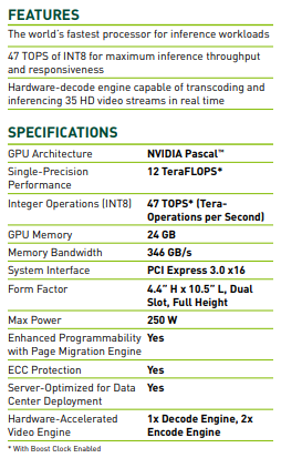
Pascal架构机型P40配置数据
NVIDIA GPU Pascal架构简述的更多相关文章
- NVIDIA GPU Volta架构简述
NVIDIA GPU Volta架构简述 本文摘抄自英伟达Volta架构官方白皮书:https://www.nvidia.com/content/dam/en-zz/Solutions/Data-Ce ...
- NVIDIA GPU Turing架构简述
NVIDIA GPU Turing架构简述 本文摘抄自Turing官方白皮书:https://www.nvidia.com/content/dam/en-zz/Solutions/design-vis ...
- 深入GPU硬件架构及运行机制
目录 一.导言 1.1 为何要了解GPU? 1.2 内容要点 1.3 带着问题阅读 二.GPU概述 2.1 GPU是什么? 2.2 GPU历史 2.2.1 NV GPU发展史 2.2.2 NV GPU ...
- Caffe Ubuntu14.04 + CUDA 8 (支持GTX1080 1070等Pascal架构显卡)
1. 前言 本教程使用的系统是Ubuntu 14.04 LTS 64-bit,使用的CUDA版本为8. 理论上本教程支持Pascal架构显卡,如游戏卡GeForce GTX1070,GTX 1080, ...
- NVIDIA Turing Architecture架构设计(下)
NVIDIA Turing Architecture架构设计(下) GDDR6 内存子系统 随着显示分辨率不断提高,着色器功能和渲染技术变得更加复杂,内存带宽和大小在 GPU 性能中扮演着更大的角色. ...
- NVIDIA Turing Architecture架构设计(上)
NVIDIA Turing Architecture架构设计(上) 在游戏市场持续增长和对更好的 3D 图形的永不满足的需求的推动下, NVIDIA 已经将 GPU 发展成为许多计算密集型应用的世界领 ...
- GPU体系架构(一):数据的并行处理
最近在了解GPU架构这方面的内容,由于资料零零散散,所以准备写两篇博客整理一下.GPU的架构复杂无比,这两篇文章也是从宏观的层面去一窥GPU的工作原理罢了 GPU根据厂商的不同,显卡型号的不同,GPU ...
- GPU体系架构(二):GPU存储体系
GPU是一个外围设备,本来是专门作为图形渲染使用的,但是随着其功能的越来越强大,GPU也逐渐成为继CPU之后的又一计算核心.但不同于CPU的架构设计,GPU的架构从一开始就更倾向于图形渲染和大规模数据 ...
- NVIDIA GPU的快速傅立叶变换
NVIDIA GPU的快速傅立叶变换 cuFFT库提供GPU加速的FFT实现,其执行速度比仅CPU的替代方案快10倍.cuFFT用于构建跨学科的商业和研究应用程序,例如深度学习,计算机视觉,计算物理, ...
随机推荐
- Nginx安装配置介绍(二)
一:Nginx安装(Windows) 官网地址:https://nginx.org/en/download.html 解压完成后,文件目录如下: 启动Nginx: 直接双击目录下的nginx.exe, ...
- 如何用 React 构建前端架构
早期的前端是由后端开发的,最开始的时候仅仅做展示,点一下链接跳转到另外一个页面去,渲染表单,再用Ajax的方式请求网络和后端交互,数据返回来还需要把数据渲染到DOM上.写这样的代码的确是很简单.在We ...
- 深入理解Java闭包概念
闭包又称词法闭包 闭包最早定义为一种包含<环境成分>和<控制成分>的实体. 解释一:闭包是引用了自由变量的函数,这个被引用的变量将和这个函数一同存在. 解释二:闭包是函数和相关 ...
- 阿里巴巴--mysql中Mysql模糊查询like效率,以及更高效的写法
在使用msyql进行模糊查询的时候,很自然的会用到like语句,通常情况下,在数据量小的时候,不容易看出查询的效率,但在数据量达到百万级,千万级的时候,查询的效率就很容易显现出来.这个时候查询的效率就 ...
- unable to load script from assets 'index.android bundle'
在Android手机上运行React-native项目时 报错:unable to load script from assets 'index.android bundle' ,make sure ...
- P2220 [HAOI2012]容易题【快速幂】
题目描述 为了使得大家高兴,小Q特意出个自认为的简单题(easy)来满足大家,这道简单题是描述如下: 有一个数列A已知对于所有的A[i]都是1~n的自然数,并且知道对于一些A[i]不能取哪些值,我们定 ...
- Spreading the Wealth
题目 A Communist regime is trying to redistribute wealth in a village. They have have decided to sit e ...
- Ubuntu apt update卡在Connecting to security.ubuntu.com解决方法
Ubuntu操作系统运行apt update命令时会卡在Connecting to security.ubuntu.com,搭了梯子也无法解决 尝试了网络上的方法,如: https://blog.cs ...
- 解决Centos7下中文显示乱码
第一步:先查看是不是ctr的问题: SecureCRT的修改,选项→会话选项,将外观中的字符编码集修改为UTF-8即可,其他终端程序同理 如果不是则再参照如下文档操作:https://www.cnbl ...
- 什么是EL表达式?
1.什么是EL表达式? EL(Expression Language) 是为了使JSP写起来更加简单.表达式语言的灵感来自于 ECMAScript 和 XPath 表达式语言,它提供了在 JSP 中简 ...